| Su | Mo | Tu | We | Th | Fr | Sa |
|---|---|---|---|---|---|---|
| Su | Mo | Tu | We | Th | Fr | Sa |
|---|---|---|---|---|---|---|


 |Sep 4, 2018|
Atomic layer etching (ALE) is one of the chipmaking processes that makes our data-driven world possible. After being confined to the laboratory for decades, ALE has awakened to become the most...
 |Jul 16, 2018|
Now that our time at SEMICON West 2018 is over, we’d like to reflect on some of the sound-bites overheard last week. As always, the three-day conference and expo gave us insights into today’s...
 |Mar 7, 2018|
Lam Research has been recognized by Intel as a recipient of a 2017 Preferred Quality Supplier (PQS) award. The PQS award recognizes companies like Lam that Intel believes have relentlessly pursued...
 |Feb 26, 2018|
Looking ahead into the new year in technology often proves quite interesting and educational. For 2018, one well-established market – automotive – is gaining the attention of many technology...
 |Jan 2, 2018|
Welcome back to the Lam Blog. We hope you had a happy and prosperous holiday season. As a prelude to what you can expect in upcoming blog stories, we wanted to highlight some of the favorite posts...
 |Dec 14, 2017|
As we start to wind down 2017, all of us at Lam would like to take this opportunity to wish our friends, colleagues, customers, and collaborators around the globe a holiday season full of warmth...
 |Sep 11, 2017|
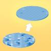
Multiple patterning continues to be an important technique for enabling pitch shrinking in advanced chip designs. However, as the number of steps grows, managing process variation is a key...
 |Jul 31, 2017|
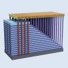
The industry’s transition to 3D NAND is being driven by several important advantages, including its ability to deliver higher capacity with a lower cost per bit. These vertical architectures...
 |Jun 12, 2017|
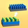
Used to extend the capabilities of conventional lithography, multiple patterning is a process of overlaying patterns of larger dimensions to achieve smaller and/or more tightly packed features. In...
 |Apr 7, 2017|
Panel-level fan-out chip manufacturing – using large square or rectangular substrates instead of wafers – is being developed as a means to lower the cost of back-end processes for some...