| Su | Mo | Tu | We | Th | Fr | Sa |
|---|---|---|---|---|---|---|
| Su | Mo | Tu | We | Th | Fr | Sa |
|---|---|---|---|---|---|---|


 |Dec 15, 2016|
As 2016 comes to a close, we thought we’d take a few moments to look back on the year as reflected in the Lam Blog. Through our stories, we shared some of our proud moments, like when the...
 |Sep 6, 2016|
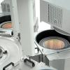
With the introduction of Lam’s latest Flex™ dielectric etch system, we have expanded our atomic layer etching (ALE) portfolio to include both conductor and dielectric etch. At the 10 nm...
 |Aug 9, 2016|
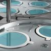
Addressing critical needs for next-generation 3D NAND and DRAM devices, Lam has developed the industry’s first all-atomic layer deposition (ALD) low-fluorine tungsten (LFW) fill process with its...
 |Aug 1, 2016|
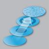
Multiple patterning is an innovative approach to scaling semiconductors, but it also poses significant challenges controlling process variations. Lam’s Rick Gottscho, executive vice president of...
 |Jul 17, 2016|
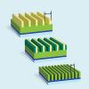
The semiconductor industry has long relied on the development of innovative device architectures and technologies to continue device scaling. Making these a reality in production, however,...