| Su | Mo | Tu | We | Th | Fr | Sa |
|---|---|---|---|---|---|---|
| Su | Mo | Tu | We | Th | Fr | Sa |
|---|---|---|---|---|---|---|


 |Sep 12, 2016|
Transistors are at the heart of our cherished electronics. Millions, or even billions, of these tiny switches go to work for us when we check our mobile phones, use our computers, start our...

 |Sep 6, 2016|
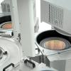
With the introduction of Lam’s latest Flex™ dielectric etch system, we have expanded our atomic layer etching (ALE) portfolio to include both conductor and dielectric etch. At the 10 nm...

 |Aug 29, 2016|
The semiconductor manufacturing community is gearing up for SEMICON Taiwan, the largest microelectronics event in Taiwan, which is expected to attract more than 40,000 visitors from around the...
 |Aug 9, 2016|
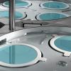
Addressing critical needs for next-generation 3D NAND and DRAM devices, Lam has developed the industry’s first all-atomic layer deposition (ALD) low-fluorine tungsten (LFW) fill process with its...
 |Aug 1, 2016|
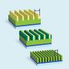
Multiple patterning is an innovative approach to scaling semiconductors, but it also poses significant challenges controlling process variations. Lam’s Rick Gottscho, executive vice president of...