| Su | Mo | Tu | We | Th | Fr | Sa |
|---|---|---|---|---|---|---|
| Su | Mo | Tu | We | Th | Fr | Sa |
|---|---|---|---|---|---|---|


 |Nov 8, 2022|
Introduction The semiconductor industry has been focused on scaling and developing advanced technologies using advanced etch tools and techniques. With decreasing semiconductor device dimensions...

 Lam Research Drives Technology Advancements for Next-Generation Semiconductors (SEMICON Taiwan 2022)|Nov 2, 2022|
Lam Research was the platinum sponsor of the 27th gathering of SEMICON Taiwan, held September 14 to 16. More than 45,000 attendees examined 2,450 exhibition booths showing the latest industry...

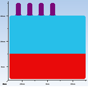
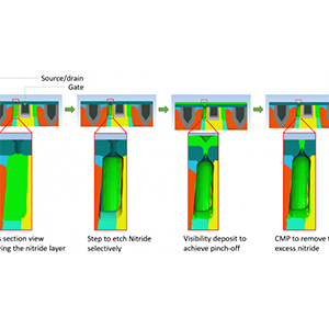 |Oct 27, 2022|
Reducing the parasitic capacitance between the gate metal and the source/drain contact of a transistor can decrease device switching delays. One way to reduce parasitic capacitance is to reduce...

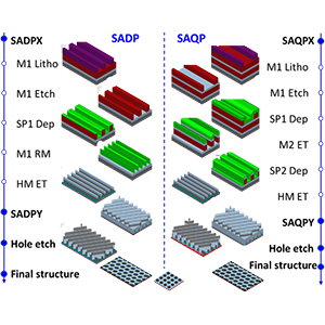 |Sep 22, 2022|
With continuous device scaling, process windows have become narrower and narrower due to smaller feature sizes and greater process step variability [1]. A key task during the R&D stage of...

 |Aug 30, 2022|
John has 25 years in the industry and 49 patents to his name Multidisciplinary skills in dep and etch have led to groundbreaking work John Drewery has been named a Lam Research Fellow for...