| Su | Mo | Tu | We | Th | Fr | Sa |
|---|---|---|---|---|---|---|
| Su | Mo | Tu | We | Th | Fr | Sa |
|---|---|---|---|---|---|---|


 |Jul 15, 2022|
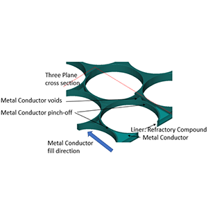
Modern semiconductor processes are extremely complicated and involve thousands of interacting individual process steps. During the development of these process steps, roadblocks and barriers are...

 |Jul 12, 2022|
And yes, we’ve got a solution for that In the recent blog article Our wireless world – how Wi-Fi 6 will seamlessly integrate with 5G to keep us connected, David Haynes from our Customer...

 |Jul 7, 2022|
Lam Research will join fellow industry leaders from the extended electronics supply chain in a range of talks at the SEMICON West 2022 hybrid conference later this month. During the 52nd annual...
 |Jun 29, 2022|
At Lam, we understand that the innovations we create will touch the lives of nearly every person on the planet. As we move the world forward with our technology, we aspire to integrate...

 |Jun 28, 2022|
On June 28, 1969, members and allies of the LGBTQIA+ community stood up for justice when police raided Stonewall Inn, a gay bar in New York City. This event galvanized LGBTQIA+ activism, and more...

 |Jun 16, 2022|
Chips are everywhere: from our mobile phones and automobiles to cloud servers for artificial intelligence, all of which seem to get faster, smarter, and better with each generation. Creating more...

 |Jun 7, 2022|
Every few months, new and improved electronics are introduced. They’re typically smaller, smarter, faster, have more bandwidth, are more power-efficient, etc. – all thanks to a new generation...

 |Jun 3, 2022|
Lam jumped 54 slots to #250 on the Fortune 500, an annual list published by Fortune magazine that ranks the largest corporations in the United States by revenue for the 2021 fiscal year. In the...

 |Jun 1, 2022|
It takes a lot of different types of process tools to make chips, from deposition, to lithographic to etch and to cleaning tools among others. Large scale production requires chipmakers to use...
 |May 17, 2022|
Welcome to our new blog series: Stepping Up, where we celebrate our manufacturing workforce by spotlighting some of the amazing people that are helping to keep Lam’s global operations and supply...