| Su | Mo | Tu | We | Th | Fr | Sa |
|---|---|---|---|---|---|---|
| Su | Mo | Tu | We | Th | Fr | Sa |
|---|---|---|---|---|---|---|


 |Jun 14, 2023|
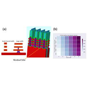
As transistor sizes shrink, short channel effects make it more difficult for transistor gates to turn a transistor ON and OFF [1]. One method to overcome this problem is to move away from planar...

 |May 30, 2023|
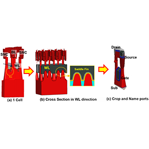
As DRAM technology nodes have scaled down, access transistor issues have been highlighted due to weak gate controllability. Saddle Fins with Buried Channel Array Transistors (BCAT) have...

 |May 25, 2023|
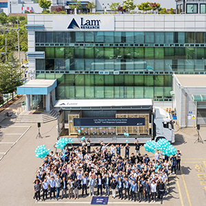
Achievement represents close collaboration with our customers and supply chain partners LMK joins Lam’s manufacturing operations in Livermore, Tualatin, and Taiwan in this milestone This week,...

 |May 2, 2023|
EVs can have almost twice as many microchips as combustion engine vehicles. Lam is a critical supplier for semiconductor manufacturers for EVs across all technologies.

 |Apr 13, 2023|
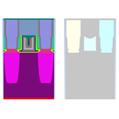
Introduction In logic devices such as FinFETs (field-effect transistors), metal gate parasitic capacitance can negatively impact electrical performance. One way to reduce this parasitic...