| Su | Mo | Tu | We | Th | Fr | Sa |
|---|---|---|---|---|---|---|
| Su | Mo | Tu | We | Th | Fr | Sa |
|---|---|---|---|---|---|---|


 |Nov 8, 2022|
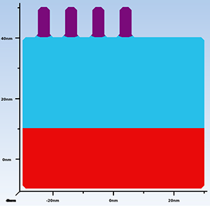
Introduction The semiconductor industry has been focused on scaling and developing advanced technologies using advanced etch tools and techniques. With decreasing semiconductor device dimensions...

 |Oct 27, 2022|
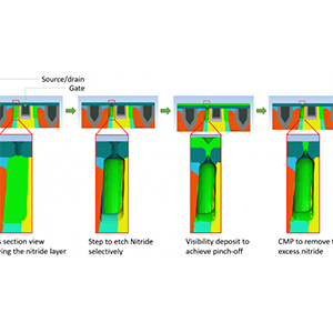
Reducing the parasitic capacitance between the gate metal and the source/drain contact of a transistor can decrease device switching delays. One way to reduce parasitic capacitance is to reduce...

 |Sep 22, 2022|
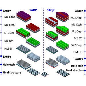
With continuous device scaling, process windows have become narrower and narrower due to smaller feature sizes and greater process step variability [1]. A key task during the R&D stage of...

 |Aug 18, 2022|
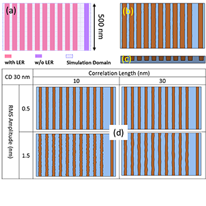
Introduction BEOL metal line RC delay has become a dominant factor that limits chip performance at advanced nodes [1]. Smaller metal line pitches require a narrower line CD and line-to-line...

 |Jul 15, 2022|
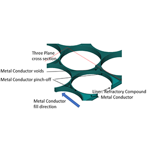
Modern semiconductor processes are extremely complicated and involve thousands of interacting individual process steps. During the development of these process steps, roadblocks and barriers are...

 |Mar 14, 2022|
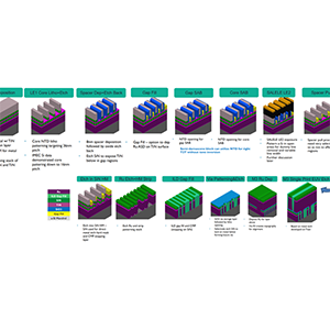
Introduction As we approach the 1.5nm node and beyond, new BEOL device integration challenges will be presented. These challenges include the need for smaller metal pitches, along with support for...
 |Feb 11, 2022|
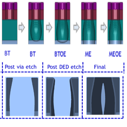
Design of Experiments (DOE) is a powerful concept in semiconductor engineering research and development. DOEs are sets of experiments used to explore the sensitivity of experimental variables and...

 |Jan 4, 2022|
When I was a small child, I remember watching a 1966 American sci-fi adventure movie called “Fantastic Voyage” (the Korean title was “Micro Squad”) on an old black-and-white TV. The...

 |Mar 8, 2021|
SEMICON China will connect technologists to the world’s fastest growing and most dynamic microelectronics market. Held at the Shanghai New International Exhibition Centre (SNIEC) on March 17-19,...

 |Oct 19, 2020|
Semiconductor process development is no easy task, with each generation of devices more difficult and expensive to create. Traditional cycles of build-and-test development are becoming obsolete,...

 |Feb 11, 2019|
The SPIE Advanced Lithography symposium brings together leaders across the semiconductor industry to discuss the latest challenges in lithography and patterning. Held at the San Jose Convention...