| Su | Mo | Tu | We | Th | Fr | Sa |
|---|---|---|---|---|---|---|
| Su | Mo | Tu | We | Th | Fr | Sa |
|---|---|---|---|---|---|---|


 |Aug 9, 2023|
Lam Research and the Centre for Nano Science and Engineering (CeNSE) at the Indian Institute of Science (IISc) partner to train up to 60,000 semiconductor engineers.

 |Jul 14, 2023|
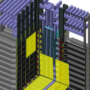
DRAM is following NAND in going 3D, but architecture needs are unique and challenging. 3D DRAM is needed to keep up with the demands of graphics cards, portable devices, and more. Here's an idea of how to architect it.

 |Jun 22, 2023|
Up to 60,000 engineers in India to be trained on Lam’s unique virtual fabrication platform
 |Jun 22, 2023|
New portfolio joins physical and virtual semiconductor worlds into a single ecosystem

 |Jun 14, 2023|
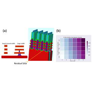
As transistor sizes shrink, short channel effects make it more difficult for transistor gates to turn a transistor ON and OFF [1]. One method to overcome this problem is to move away from planar...

 |May 30, 2023|
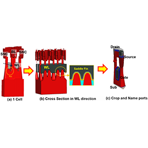
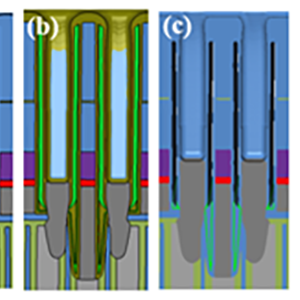
As DRAM technology nodes have scaled down, access transistor issues have been highlighted due to weak gate controllability. Saddle Fins with Buried Channel Array Transistors (BCAT) have...

 |Apr 13, 2023|
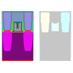
Introduction In logic devices such as FinFETs (field-effect transistors), metal gate parasitic capacitance can negatively impact electrical performance. One way to reduce this parasitic...

 |Mar 22, 2023|
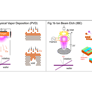
Introduction Cu’s resistivity depends on its crystal structure, void volume, grain boundaries and material interface mismatch, which becomes more significant at smaller scales. The formation of...

 |Feb 28, 2023|
With decreasing dynamic random-access memory (DRAM) cell sizes, DRAM process development has become increasingly difficult. Bit-line (BL) sensing margins and refresh times have become problematic...

 |Feb 16, 2023|
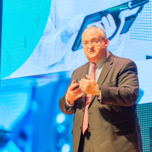
SEMICON Korea 2023 kicked off with a keynote speech, “Accelerating Innovation – From Lab to Fab,” delivered by Pat Lord, EVP of the Customer Support Business Group and Global Operations. Pat...