| Su | Mo | Tu | We | Th | Fr | Sa |
|---|---|---|---|---|---|---|
| Su | Mo | Tu | We | Th | Fr | Sa |
|---|---|---|---|---|---|---|


 |Dec 12, 2016|
This year marks the 40th anniversary for SEMICON Japan, one of the most extensive international exhibitions of semiconductor equipment and materials. Each SEMI tradeshow has its own unique...

 |Nov 28, 2016|
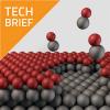
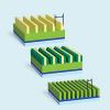
Did you know that different patterns require different types of multiple patterning? Today’s advanced chips are more complex than ever before, with transistors and other structures that are...

 |Nov 14, 2016|
Greek philosopher Democritus (460-370 BC) first proposed the existence of an ultimate particle, which he described as “atomos.” He probably never dreamed that one day there would be devices so...
 |Nov 7, 2016|
State-of-the-art advances in plasma research and thin film science will be discussed at the AVS 63rd International Symposium and Exhibition, being held November 6-11 in Nashville, Tennessee. This...
 |Sep 26, 2016|
Electrochemistry and solid-state science and technology will come together at the PRiME 2016 Meeting, held October 2-7 in Honolulu, Hawaii. One of the largest research conferences in the world,...

 |Sep 12, 2016|
Transistors are at the heart of our cherished electronics. Millions, or even billions, of these tiny switches go to work for us when we check our mobile phones, use our computers, start our...

 |Sep 6, 2016|
With the introduction of Lam’s latest Flex™ dielectric etch system, we have expanded our atomic layer etching (ALE) portfolio to include both conductor and dielectric etch. At the 10 nm...
 |Aug 29, 2016|
The semiconductor manufacturing community is gearing up for SEMICON Taiwan, the largest microelectronics event in Taiwan, which is expected to attract more than 40,000 visitors from around the...
 |Aug 9, 2016|
Addressing critical needs for next-generation 3D NAND and DRAM devices, Lam has developed the industry’s first all-atomic layer deposition (ALD) low-fluorine tungsten (LFW) fill process with its...
 |Aug 1, 2016|
Multiple patterning is an innovative approach to scaling semiconductors, but it also poses significant challenges controlling process variations. Lam’s Rick Gottscho, executive vice president of...