| Su | Mo | Tu | We | Th | Fr | Sa |
|---|---|---|---|---|---|---|
| Su | Mo | Tu | We | Th | Fr | Sa |
|---|---|---|---|---|---|---|


 |Oct 5, 2022|
Solar power generation helps move Lam toward net zero emissions goal Lam’s Malaysia operations opened in August 2020; 1,400+ employees work there Lam’s purpose is simple: Unleash the power of...

 |Sep 22, 2022|
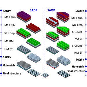
With continuous device scaling, process windows have become narrower and narrower due to smaller feature sizes and greater process step variability [1]. A key task during the R&D stage of...
 |Sep 21, 2022|
Soon oversees Lam’s Malaysia operations and 1,400+ employees Lam Research provides many opportunities to grow your career, she says Soon Kuek joined Lam Research 16 years ago in Fremont. Today...
 |Sep 20, 2022|
Alyson’s “accidental career path” went from family therapy fantasies to running IT ops Getting rid of impostor syndrome is one piece of advice she gives to young women “I run the internal...

 |Sep 14, 2022|
The India Center for Engineering (ICE) is Lam’s fifth R&D lab worldwide ICE enables the success of our customers globally by improving speed to solution Today, Lam Research held the grand...

 |Sep 8, 2022|
Calling all innovative entrepreneurs working on sustainability solutions The winner will be offered a $250,000 SAFE investment Theme is “Engineering a Greener Fab” Heatwaves such as the one...
 |Aug 30, 2022|
John has 25 years in the industry and 49 patents to his name Multidisciplinary skills in dep and etch have led to groundbreaking work John Drewery has been named a Lam Research Fellow for...

 |Aug 25, 2022|
Connect with us through our new Social Impact Program! What does it mean to have a “social impact”? For us at Lam Research, it means building meaningful partnerships with organizations that...

 |Aug 18, 2022|
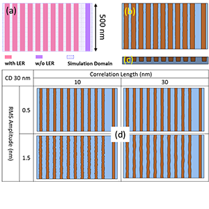
Introduction BEOL metal line RC delay has become a dominant factor that limits chip performance at advanced nodes [1]. Smaller metal line pitches require a narrower line CD and line-to-line...

 |Aug 17, 2022|
At Lam, we operate at the atomic scale—etching and depositing materials onto silicon wafers more than 10,000 times smaller than the size of objects that can be seen with the naked eye....