| Su | Mo | Tu | We | Th | Fr | Sa |
|---|---|---|---|---|---|---|
| Su | Mo | Tu | We | Th | Fr | Sa |
|---|---|---|---|---|---|---|


 |Apr 23, 2024|
Lam plays a significant role in plasma science by collaborating with researchers, supporting the Allis Prize, and employing physics, chemistry, and engineering students and experts.
-
 |Apr 22, 2024|
A key component of Lam’s strategy is improving the energy efficiency of our products

 |Apr 16, 2024|
Abstract In this article, we demonstrate a pathfinding technique for a novel Vertical DRAM technology. First, we identify important process parameters (defined by current semiconductor production...

 |Apr 12, 2024|
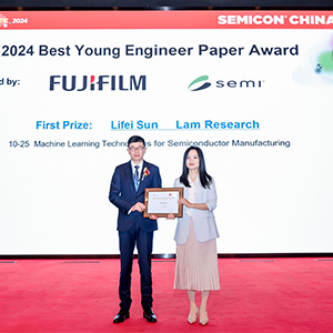
Li Fei Sun won for her paper on smart tools and ML solutions in semiconductor manufacturing In the past four years, Lam engineers have won the top award three times At Lam Research, we take pride...
-
 |Mar 26, 2024|
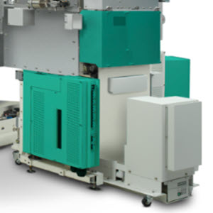
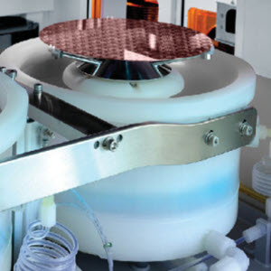
Introducing Pulsus, Lam's cutting-edge pulsed laser deposition tool. PLD enables specialty technologies like RF filters and MEMS microphones.
-
 |Mar 21, 2024|
There are still many challenges to be overcome before CFET designs become mainstream, but this new 3D architecture represents a promising new direction for the future of computing.
-
 |Mar 19, 2024|
Interest in artificial intelligence is driving data storage expansion for memory makers. Advancements in semiconductor manufacturing etch and deposition, and advanced packaging are playing a...
 |Mar 11, 2024|
One-of-a-kind contest supports semiconductor startups with investment and exposure
 |Mar 4, 2024|
Driving the news: Lam was named one of the World’s Most Ethical Companies® by Ethisphere–for the second year in a row. Lam is the only wafer fabrication equipment provider on this year’s...
-
 |Mar 1, 2024|
Dee’s career journey took on unexpected roles in engineering, quality, and operations She oversees the manufacturing operations across two facilities at Silfex I didn’t plan to work in...
-
 |Feb 28, 2024|
Explore more stories in the 'I Am Lam' video series: How Quinton McNeil Found Meaningful Work and a Community Houda Hadiji’s Resilient Career Path

 |Feb 22, 2024|
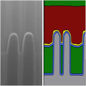
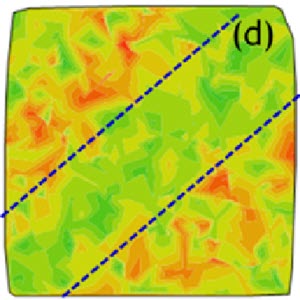
On the use and benefits of virtual fabrication in the development of DRAM saddle fin profiles
-
 |Feb 6, 2024|
JUST Capital and CNBC named Lam to the top 50 of its annual JUST 100 list.
 |Feb 5, 2024|
Lam Research has once again been named as one of Fortune’s World’s Most Admired Companies. This year, Lam ranked fourth on the global semiconductor industry rankings and #183 overall. 2024...
-
 |Feb 1, 2024|
On the use of molybdenum as a promising candidate to replace tungsten in the semiconductor industry to keep pace with Moore's Law
-
 |Jan 23, 2024|
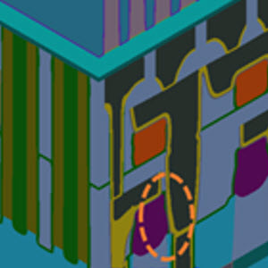
We explore the causes and implications of asymmetric wafer defects in semiconductor manufacturing. We also consider the use of virtual process modeling to understand and mitigate these structural failures.
-
 |Jan 18, 2024|
Semiconductor manufacturers scale new heights as they embrace vertical integration. Lam’s Metior succeeds where optical measuring falls short.

 |Dec 12, 2023|
The potential of Resistive Random Access Memory (ReRAM) as an alternative to SRAM for on-chip memory in advanced CPU applications.
 |Dec 5, 2023|
In a year when the semiconductor ecosystem was in the spotlight, Lam etched a mark on the industry landscape. From groundbreaking advancements in semiconductor manufacturing to progress in...

 |Nov 20, 2023|
Virtual process development tools can accelerate the identification of process hotspots. These techniques lead to cost savings and improved yields in chip manufacturing.
 |Nov 16, 2023|
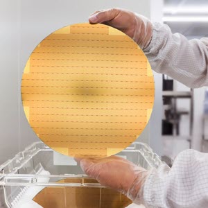
Nearly all microchips begin as slices of highly purified silicon.
 |Nov 8, 2023|
Colleen enlisted in the U.S. Navy at the age of 18 right after high school She applied her experience of equipping ships in the Pacific Ocean to Lam’s supply chain In recognition of Veterans...
-
 |Nov 8, 2023|
Summary: The rise of Artificial Intelligence (AI) has placed significant demands on semiconductor performance, particularly in the realm of etching technology. AI requires massive amounts of data...

 |Oct 25, 2023|
Enables more efficient process development via high-fidelity plasma simulation

 |Oct 19, 2023|
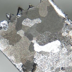
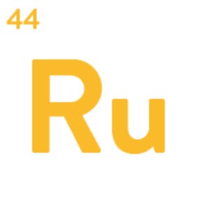
The semiconductor industry is searching for alternative metal line materials to replace copper due to the increasing barrier size and resistivity issues. Ruthenium (Ru) has shown promise as a potential replacement, outperforming copper and cobalt (Co) at smaller dimensions.
 |Oct 6, 2023|
Ammar was raised in a rural village in Malaysia FIRST® Global has given him the opportunity to dream beyond his geographical roots Ammar Akhmal wants to be a computer scientist. It’s a big...
 |Sep 28, 2023|
Related articles: Why Lam Research Is Investing in India Lam Unveils New Technology Center

 |Sep 26, 2023|
Virtual fabrication is a powerful tool to perform sensitivity analysis and provide guidance for inline process spec control

 |Sep 18, 2023|
Interns joined our sites across the globe to contribute to critical projects They took over our operations in field service, engineering, and manufacturing Every summer, I’m energized by our...
-
 |Sep 14, 2023|
Lam Research has supported the National GEM Consortium and GEM interns since 2019. Students who complete their fellowship have a chance to join Lam full-time.

 |Aug 31, 2023|
Video games and virtual and augmented reality are driving demand for haptics. Lam’s pulsed laser deposition capability can enable next-gen haptics technology.

 |Aug 23, 2023|
BEOL module processing faces challenges as chipmakers move to the 3 nm node and beyond. A semi-damascene integration scheme with airgap structures may help reduce RC delay time.

 |Aug 9, 2023|
Lam Research and the Centre for Nano Science and Engineering (CeNSE) at the Indian Institute of Science (IISc) partner to train up to 60,000 semiconductor engineers.
 |Aug 7, 2023|
The terms “fab” and “foundry” are often used interchangeably, but that’s technically incorrect. Knowing the difference is important so you can better understand the semiconductor ecosystem.

 |Jul 18, 2023|
The semiconductor industry may double in size. The environmental impact can’t increase at the same rate.

 |Jul 14, 2023|
DRAM is following NAND in going 3D, but architecture needs are unique and challenging. 3D DRAM is needed to keep up with the demands of graphics cards, portable devices, and more. Here's an idea of how to architect it.

 |Jun 30, 2023|
As we recognize Pride Month throughout June alongside the LGBTQ+ community, the topic of allyship comes up a lot. My allyship journey began in third grade when my principal, Mrs. Carroll,...
-
 |Jun 27, 2023|
Close collaboration with customers leads to rapid and predictable achievement of cost goals.
-
 |Jun 26, 2023|
This video is part of Lam’s Pride Month story collection, which amplifies the voices of employees embracing equity across the company.

 |Jun 23, 2023|
Priscilla is the platform tool owner for Lam’s dielectric etch Sense.i tools She brought her childhood passion for problem-solving to our customers’ chipmaking fabs In celebration of...
 |Jun 22, 2023|
Up to 60,000 engineers in India to be trained on Lam’s unique virtual fabrication platform
 |Jun 22, 2023|
New portfolio joins physical and virtual semiconductor worlds into a single ecosystem
-
 |Jun 20, 2023|
Addresses key manufacturing challenges and significantly improves wafer yield Builds on Lam's 15-year heritage of innovation in bevel solutions

 |Jun 14, 2023|
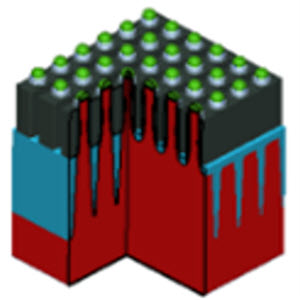
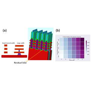
As transistor sizes shrink, short channel effects make it more difficult for transistor gates to turn a transistor ON and OFF [1]. One method to overcome this problem is to move away from planar...
 |Jun 13, 2023|
For the seventh year in a row, Lam was ranked on the Fortune 500, coming in at #240 with more than $17.2 billion in revenue. Since first debuting on the Fortune 500 at #491 in 2016, Lam has jumped...
 |May 30, 2023|
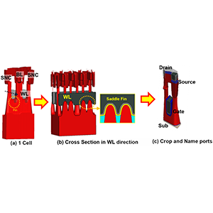
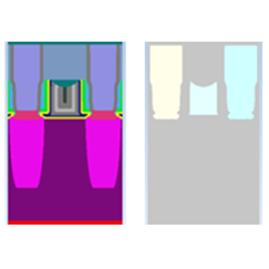
As DRAM technology nodes have scaled down, access transistor issues have been highlighted due to weak gate controllability. Saddle Fins with Buried Channel Array Transistors (BCAT) have...

 |May 25, 2023|
Achievement represents close collaboration with our customers and supply chain partners LMK joins Lam’s manufacturing operations in Livermore, Tualatin, and Taiwan in this milestone This week,...
 |May 10, 2023|
Lam Research has won a prestigious Edison Award for best new products in materials science. The bronze medal was awarded for our recently launched innovative suite of selective etch products...
 |May 2, 2023|
EVs can have almost twice as many microchips as combustion engine vehicles. Lam is a critical supplier for semiconductor manufacturers for EVs across all technologies.

 |Apr 13, 2023|
Introduction In logic devices such as FinFETs (field-effect transistors), metal gate parasitic capacitance can negatively impact electrical performance. One way to reduce this parasitic...