| Su | Mo | Tu | We | Th | Fr | Sa |
|---|---|---|---|---|---|---|
| Su | Mo | Tu | We | Th | Fr | Sa |
|---|---|---|---|---|---|---|


 |Apr 16, 2024|
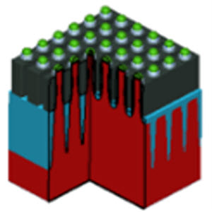
Abstract In this article, we demonstrate a pathfinding technique for a novel Vertical DRAM technology. First, we identify important process parameters (defined by current semiconductor production...

 |Apr 12, 2024|
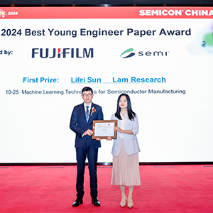
Li Fei Sun won for her paper on smart tools and ML solutions in semiconductor manufacturing In the past four years, Lam engineers have won the top award three times At Lam Research, we take pride...
-
 |Mar 26, 2024|
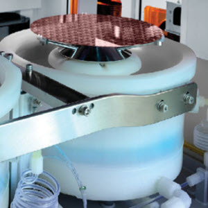
Introducing Pulsus, Lam's cutting-edge pulsed laser deposition tool. PLD enables specialty technologies like RF filters and MEMS microphones.
-
 |Mar 21, 2024|
There are still many challenges to be overcome before CFET designs become mainstream, but this new 3D architecture represents a promising new direction for the future of computing.
-
 |Mar 19, 2024|
Interest in artificial intelligence is driving data storage expansion for memory makers. Advancements in semiconductor manufacturing etch and deposition, and advanced packaging are playing a...

 |Mar 11, 2024|
One-of-a-kind contest supports semiconductor startups with investment and exposure
 |Mar 4, 2024|
Driving the news: Lam was named one of the World’s Most Ethical Companies® by Ethisphere–for the second year in a row. Lam is the only wafer fabrication equipment provider on this year’s...
-
 |Mar 1, 2024|
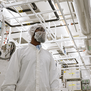
Dee’s career journey took on unexpected roles in engineering, quality, and operations She oversees the manufacturing operations across two facilities at Silfex I didn’t plan to work in...
-
 |Feb 28, 2024|
Explore more stories in the 'I Am Lam' video series: How Quinton McNeil Found Meaningful Work and a Community Houda Hadiji’s Resilient Career Path

 |Feb 22, 2024|
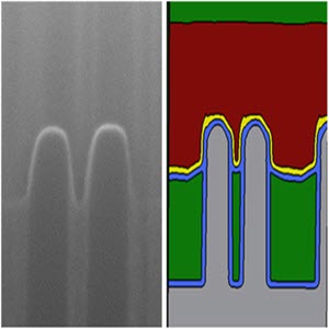
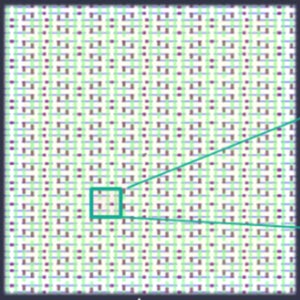
On the use and benefits of virtual fabrication in the development of DRAM saddle fin profiles
-
 |Feb 6, 2024|
JUST Capital and CNBC named Lam to the top 50 of its annual JUST 100 list.
 |Feb 5, 2024|
Lam Research has once again been named as one of Fortune’s World’s Most Admired Companies. This year, Lam ranked fourth on the global semiconductor industry rankings and #183 overall. 2024...
-
 |Feb 1, 2024|
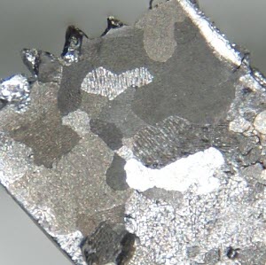
On the use of molybdenum as a promising candidate to replace tungsten in the semiconductor industry to keep pace with Moore's Law
-
 |Jan 23, 2024|
We explore the causes and implications of asymmetric wafer defects in semiconductor manufacturing. We also consider the use of virtual process modeling to understand and mitigate these structural failures.
-
 |Jan 18, 2024|
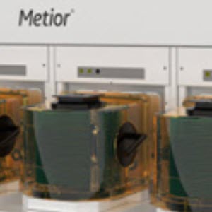
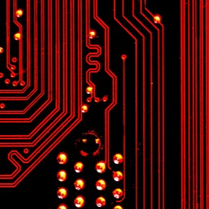
Semiconductor manufacturers scale new heights as they embrace vertical integration. Lam’s Metior succeeds where optical measuring falls short.

 |Dec 12, 2023|
The potential of Resistive Random Access Memory (ReRAM) as an alternative to SRAM for on-chip memory in advanced CPU applications.
 |Dec 5, 2023|
In a year when the semiconductor ecosystem was in the spotlight, Lam etched a mark on the industry landscape. From groundbreaking advancements in semiconductor manufacturing to progress in...

 |Nov 20, 2023|
Virtual process development tools can accelerate the identification of process hotspots. These techniques lead to cost savings and improved yields in chip manufacturing.
 |Nov 16, 2023|
Nearly all microchips begin as slices of highly purified silicon.
 |Nov 8, 2023|
Colleen enlisted in the U.S. Navy at the age of 18 right after high school She applied her experience of equipping ships in the Pacific Ocean to Lam’s supply chain In recognition of Veterans...
-
 |Nov 8, 2023|
Summary: The rise of Artificial Intelligence (AI) has placed significant demands on semiconductor performance, particularly in the realm of etching technology. AI requires massive amounts of data...

 |Oct 25, 2023|
Enables more efficient process development via high-fidelity plasma simulation

 |Oct 19, 2023|
The semiconductor industry is searching for alternative metal line materials to replace copper due to the increasing barrier size and resistivity issues. Ruthenium (Ru) has shown promise as a potential replacement, outperforming copper and cobalt (Co) at smaller dimensions.
 |Oct 6, 2023|
Ammar was raised in a rural village in Malaysia FIRST® Global has given him the opportunity to dream beyond his geographical roots Ammar Akhmal wants to be a computer scientist. It’s a big...
 |Sep 28, 2023|
Related articles: Why Lam Research Is Investing in India Lam Unveils New Technology Center