| Su | Mo | Tu | We | Th | Fr | Sa |
|---|---|---|---|---|---|---|
| Su | Mo | Tu | We | Th | Fr | Sa |
|---|---|---|---|---|---|---|

-
 |May 14, 2024|
As semiconductor complexity increases with scaling, specialized expertise in areas like plasma physics and artificial intelligence (AI) becomes crucial. Lam faces challenges in workforce...

 |Apr 16, 2024|
Abstract In this article, we demonstrate a pathfinding technique for a novel Vertical DRAM technology. First, we identify important process parameters (defined by current semiconductor production...

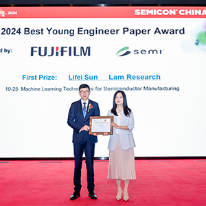 |Apr 12, 2024|
Li Fei Sun won for her paper on smart tools and ML solutions in semiconductor manufacturing In the past four years, Lam engineers have won the top award three times At Lam Research, we take pride...
-
 |Mar 21, 2024|
There are still many challenges to be overcome before CFET designs become mainstream, but this new 3D architecture represents a promising new direction for the future of computing.

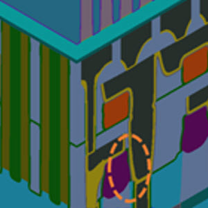
 |Feb 22, 2024|
On the use and benefits of virtual fabrication in the development of DRAM saddle fin profiles
-
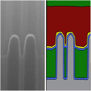
 |Jan 23, 2024|
We explore the causes and implications of asymmetric wafer defects in semiconductor manufacturing. We also consider the use of virtual process modeling to understand and mitigate these structural failures.

 |Dec 12, 2023|
The potential of Resistive Random Access Memory (ReRAM) as an alternative to SRAM for on-chip memory in advanced CPU applications.

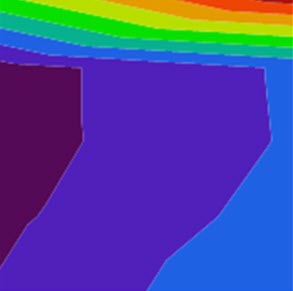
 |Nov 20, 2023|
Virtual process development tools can accelerate the identification of process hotspots. These techniques lead to cost savings and improved yields in chip manufacturing.

 |Sep 26, 2023|
Virtual fabrication is a powerful tool to perform sensitivity analysis and provide guidance for inline process spec control

 |Aug 23, 2023|
BEOL module processing faces challenges as chipmakers move to the 3 nm node and beyond. A semi-damascene integration scheme with airgap structures may help reduce RC delay time.