| Su | Mo | Tu | We | Th | Fr | Sa |
|---|---|---|---|---|---|---|
| Su | Mo | Tu | We | Th | Fr | Sa |
|---|---|---|---|---|---|---|


 |Nov 16, 2023|
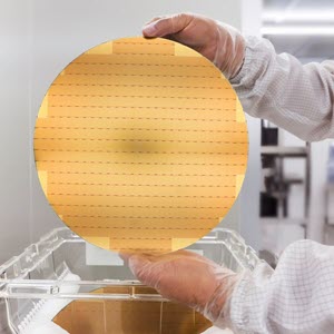
Nearly all microchips begin as slices of highly purified silicon.
 |Aug 7, 2023|
The terms “fab” and “foundry” are often used interchangeably, but that’s technically incorrect. Knowing the difference is important so you can better understand the semiconductor ecosystem.
 |May 10, 2023|
Lam Research has won a prestigious Edison Award for best new products in materials science. The bronze medal was awarded for our recently launched innovative suite of selective etch products...

 |Apr 5, 2023|
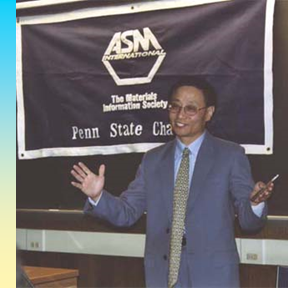
Hong Shih is one of 10 employees within the company who has been elevated to Lam Fellow He has more than 40 years of experience in sciences and engineering with over 30 years working in the...
 |Mar 7, 2023|
Gosia’s redirection in her studies resulted in a 20+ year long career in semiconductors A little bit of luck and a whole lot of talent got her to where she is today I sat down with Gosia...

 |Feb 16, 2023|
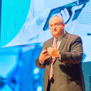
SEMICON Korea 2023 kicked off with a keynote speech, “Accelerating Innovation – From Lab to Fab,” delivered by Pat Lord, EVP of the Customer Support Business Group and Global Operations. Pat...

 Lam Research Drives Technology Advancements for Next-Generation Semiconductors (SEMICON Taiwan 2022)|Nov 2, 2022|
Lam Research was the platinum sponsor of the 27th gathering of SEMICON Taiwan, held September 14 to 16. More than 45,000 attendees examined 2,450 exhibition booths showing the latest industry...

 |Sep 8, 2022|
Calling all innovative entrepreneurs working on sustainability solutions The winner will be offered a $250,000 SAFE investment Theme is “Engineering a Greener Fab” Heatwaves such as the one...

 |Jul 21, 2022|
The electronics supply chain recently gathered together at SEMICON Southeast Asia, a premier event that promotes growth of the semiconductor and microelectronics ecosystem in the region. Held June...

 |Jul 12, 2022|
And yes, we’ve got a solution for that In the recent blog article Our wireless world – how Wi-Fi 6 will seamlessly integrate with 5G to keep us connected, David Haynes from our Customer...
 |Jul 7, 2022|
Lam Research will join fellow industry leaders from the extended electronics supply chain in a range of talks at the SEMICON West 2022 hybrid conference later this month. During the 52nd annual...

 |Jun 7, 2022|
Every few months, new and improved electronics are introduced. They’re typically smaller, smarter, faster, have more bandwidth, are more power-efficient, etc. – all thanks to a new generation...

 |Jun 1, 2022|
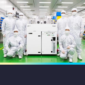
It takes a lot of different types of process tools to make chips, from deposition, to lithographic to etch and to cleaning tools among others. Large scale production requires chipmakers to use...
 |May 2, 2022|
David Haynes, vice president of Specialty Technologies for the Customer Support Business Group (CSBG) at Lam Research, discusses the introduction of Wi-Fi 6 and how, together with 5G, it will...
 |Nov 18, 2021|
Once considered to be science fiction and fodder for Hollywood films, artificial intelligence (AI) has become a near-ubiquitous technology in our communities, homes and workplaces that is helping...
 |Oct 11, 2021|
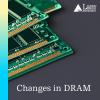
The ability to process data is foundational to our smart, connected world. Microprocessors, in turn, rely on memory chips to store the data they need while working. One of the most popular types...
 |Aug 9, 2021|
As a materials engineer, I am very proud of the fact that key advances in human civilization have been driven by materials innovation. The stone age, bronze age and iron age were all essential...
 |Jul 26, 2021|
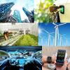
There’s a lot of talk about the Internet of Things (IoT) and its impact on our day-to-day lives. From home security systems to smart watches, IoT is upgrading the technologies we rely on every...
 |Jun 1, 2021|
We take microprocessors for granted. Most people who aren’t deeply involved in technology may have no idea all of the places where a microprocessor shows up in their lives. It’s not just their...
 |Apr 26, 2021|
The excitement around the rollout of 5G technology could not be more palpable. We see this next-generation technology in news headlines and commercials, with promises to usher in the next wave of...
 |Jan 4, 2021|
To kick-off the new year, we thought we’d share some of our favorite stories from 2020. While not exhaustive, this short list features articles that help put technology concepts into perspective...

 |Nov 25, 2020|
The 22nd Electronics Packaging Technology Conference (EPTC) is going virtual this year. The flagship event of the IEEE Electronics Packaging Society (EPS) in Region 10 will highlight technical...
 |Nov 23, 2020|
The movement of money has undergone substantial changes over the years. With the advent of financial technology, or FinTech, the financial services industry has transformed. Enabled by today’s...
 |Oct 5, 2020|
Semiconductors can be considered as one of the most important inventions of all time. They are foundational to our ability to connect with each other; to collect, store and process information;...
 |Sep 28, 2020|
Cities around the globe are experiencing software updates – swapping out antiquated data collection techniques for new technological initiatives to promote efficiency, transparency, and...