| Su | Mo | Tu | We | Th | Fr | Sa |
|---|---|---|---|---|---|---|
| Su | Mo | Tu | We | Th | Fr | Sa |
|---|---|---|---|---|---|---|


 |Nov 11, 2022|
On November 11, we observe Veterans Day in the United States, an annual holiday recognizing those who have served in the armed forces and have made a significant commitment to their country. We...

 |Nov 9, 2022|
I was thrilled to attend the FIRST Global Challenge in Geneva in October, where Lam was a Gold Sponsor. The competition arena was full of high-school students, but I was the one who got an education.

 |Nov 8, 2022|
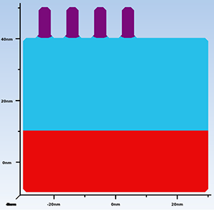
Introduction The semiconductor industry has been focused on scaling and developing advanced technologies using advanced etch tools and techniques. With decreasing semiconductor device dimensions...

 |Nov 7, 2022|
12 suppliers were awarded 2022 Supplier Excellence awards Suppliers demonstrated success across three award categories: scaling, resiliency, and rapid prototype materials performance On Thursday,...

 Lam Research Drives Technology Advancements for Next-Generation Semiconductors (SEMICON Taiwan 2022)|Nov 2, 2022|
Lam Research was the platinum sponsor of the 27th gathering of SEMICON Taiwan, held September 14 to 16. More than 45,000 attendees examined 2,450 exhibition booths showing the latest industry...

 |Oct 27, 2022|
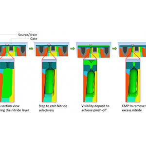
Reducing the parasitic capacitance between the gate metal and the source/drain contact of a transistor can decrease device switching delays. One way to reduce parasitic capacitance is to reduce...

 |Oct 17, 2022|
Lam launches 3-year partnership with FIRST Global to help inspire future innovators around the world Volunteers signed up to mentor robotics teams around the world for the FIRST Global Challenge...

 |Oct 12, 2022|
From supply chain to engineering, Lam’s internships offer an opportunity to gain valuable, real-world experience This year, our interns supported projects that will help move our solutions...

 |Oct 7, 2022|
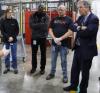
Silfex was founded in 1971, the same year “Silicon Valley” was coined ~1,400 employees work across two locations in Ohio Just in time to honor Manufacturing Day, U.S. Sen. Sherrod Brown met...
 |Oct 6, 2022|
We’ve rolled out programs that improve our benefits and reinforce our culture Lam remains committed to building a culture that is inclusive and diverse In celebration of Global Diversity...