| Su | Mo | Tu | We | Th | Fr | Sa |
|---|---|---|---|---|---|---|
| Su | Mo | Tu | We | Th | Fr | Sa |
|---|---|---|---|---|---|---|


 |Sep 29, 2026|
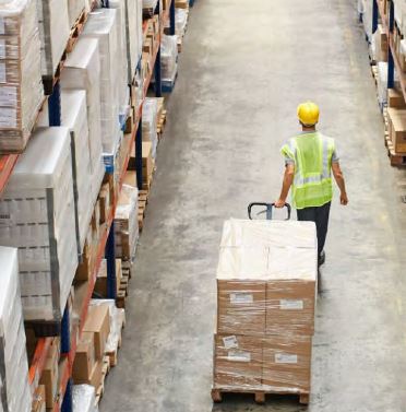
Lam Research’s new Silicon Valley warehouse speeds semiconductor parts retrieval and strengthens U.S. supply chain resilience.
 |Sep 8, 2026|
AI is increasing demand for larger and more complex chip packages. Traditional wafer-based packaging faces scaling challenges for large-format designs. Panel-level processing may improve...
 |Aug 31, 2026|
Lam Research broke ground on a new advanced R&D lab in Tualatin, Oregon, expanding cleanroom capacity and strengthening its global lab network.
 |Jul 21, 2026|
SABRE 3D is an electrochemical deposition solution engineered for precision copper plating (the critical wiring of modern semiconductor devices).
 |Jul 9, 2026|
AI is redefining semiconductor scaling Audrey Charles discusses the technologies, partnerships, and innovations that will define the future of semiconductor scaling AI is driving unprecedented...
 |Jul 2, 2026|
A Lam scanning electron microscope technician shares how he started a career at Lam Research and continues his journey today as a lab supervisor.
 |Jun 18, 2026|
See how Lam’s dry resist technology helps enable the precision, flexibility, and efficiency needed for next-generation EUV chipmaking.
 |Jun 8, 2026|
Driving the news: Lam Research moved up the Fortune 500, reflecting strong revenue in Lam’s most recent fiscal year as demand for advanced semiconductor accelerates in the AI era. Lam ranked 238...
 |May 27, 2026|
The 2026 Lam Capital Venture Competition highlighted breakthrough semiconductor innovations with Lightfinder winning for its chip-scale optical sensing technology designed to enable real-time, in-tool metrology. This event showcased Lam Research's leadership in supporting startups that build the AI backbone for semiconductor manufacturing.
 |May 7, 2026|
As semiconductor manufacturing grows more complex, sensor‑driven intelligence is emerging as a critical enabler of autonomous, data‑driven fabs.
 |Apr 27, 2026|
Lam Research won two prestigious 2026 Edison Awards, for ALTUS® Halo and Akara®
 |Apr 8, 2026|
In this edition of Semi 101, we explore the evolution of transistor architectures that have enabled logic scaling.
 |Mar 19, 2026|
Integrity isn’t optional at Lam, and this latest recognition underscores that commitment.
 |Mar 17, 2026|
IBM and Lam Research have partnered in a five-year collaboration to develop processes that enable logic chip scaling beyond the 1nm node using high-NA EUV lithography.
 |Mar 10, 2026|
The 2026 Lam Capital Venture Competition is a unique event that connects semiconductor startups with industry leaders, investors, and technical experts to advance AI-enabled semiconductor technologies.
 |Feb 24, 2026|
With AI's overwhelming demand for DRAM, Lam is accelerating its response with streamlined workflows and specialized tools help speed efficiency, yield, and cost savings.
 |Feb 19, 2026|
As a viable alternative to silicon, gallium nitride (GaN) can help data centers meet the growing demands of AI by enabling more efficient power delivery and reducing energy consumption.
 |Feb 13, 2026|
DRAM scaling has reached the angstrom level—and the advanced architectures and processes that make higher performance and lower cost per bit possible. Watch now to see how memory keeps getting smaller.
 |Feb 12, 2026|
Lam Research and CEA-Leti have formed a multi-year partnership to accelerate the development of specialty technology devices critical for AI hardware. This collaboration focuses on advancing materials, processes, and manufacturable solutions to improve energy efficiency and performance in AI data centers.
 |Feb 11, 2026|
Lam Research’s Aether dry resist technology eliminates pattern collapse and reduces defects, enabling precise, high‑aspect‑ratio features for next‑generation 3D DRAM and HBM.
 |Feb 5, 2026|
With over 40 years in making semiconductor equipment, Lam Research has demonstrated leadership in etch and deposition that meet the precision and yield demands of advanced packaging, helping customers ramp new technologies with confidence.
 |Jan 23, 2026|
Lam’s Aether® dry‑resist technology plays a key role in enabling next-gen logic chips, including the latest 2 nm node
 |Jan 23, 2026|
Fortune has named Lam to its World’s Most Admired Companies list for 2026.
 |Jan 12, 2026|
DRAM is volatile memory that has the advantages of simplicity and high density. Lam is continuously innovating for each DRAM inflection as data-intensive AI requires more and more data at higher speeds.
 |Jan 8, 2026|
Lam Research improved its CDP Climate Change score from B to A-, reflecting progress toward our net zero goal and commitment to transparency.
 |Jan 7, 2026|
Lam’s newest innovation, the VECTOR® TEOS 3D tool, is crafted at its Tualatin, Oregon facility by a talented local workforce known for its multidisciplinary expertise. The company’s strong commitment to employee safety, career satisfaction, and professional growth has resulted in an outstanding retention rate, making Tualatin a standout example of manufacturing excellence.
 |Dec 9, 2025|
Watch the video on the next wave of semiconductor innovation with advanced packaging solutions from Lam Research.
 |Dec 8, 2025|
Micron awarded Lam for exceptional performance in front-end equipment supply.
 |Nov 21, 2025|
Lam Research’s latest milestone in its global expansion is in Tualatin, Oregon. The development signals what’s next for Oregon, the Silicon Forest, and the future of American leadership in the semiconductor industry.
 |Nov 17, 2025|
Startup backed by Lam Capital reduces metal contaminated liquid waste by up to 90%
 |Nov 5, 2025|
Molybdenum hybrid metallization is driving innovation in semiconductor materials for AI, 5G, and data centers. These advances boost performance, sustainability, and efficiency in chip manufacturing.
 |Nov 3, 2025|
As a founding donor of the Semiconductor Pathways Fund, Lam Research is taking action to ensure promising STEM students can complete their degrees and power the next generation...
 |Oct 30, 2025|
As Moore’s Law slows, advanced semiconductor packaging techniques are being adopted to integrate multiple chip types like logic, memory, and I/O into a single package, enhancing performance and cost-efficiency.
 |Oct 29, 2025|
Cooperative robots take center stage at FIRST Global in Panama Lam is a pioneer in semi mechatronics, like Dextro
 |Oct 29, 2025|
Students at a growing number of U.S. schools learn the “why” of advanced 3D processes SEMulator3D® helps students with immersive training on leading edge technologies.
 |Oct 21, 2025|
Lam CVP David Fried explains how Fabtex Yield Optimizer is the newest Semiverse Solutions technology to help the semiconductor industry achieve higher yields
 |Oct 16, 2025|
an in-depth look at the challenges facing the industry as AI, memory, and logic demands accelerate
 |Oct 14, 2025|
The Colorado School of Mines award is given to its most generous contributors Research investigates ways to improve etch selectivity, thermal ALD, and more Share this news with your network
 |Oct 8, 2025|
Lam Research earned the 2025 SEMI Award for North America for our pioneering cryogenic etch technology
 |Oct 7, 2025|
Fabtex™ Yield Optimizer is a new Semiverse® Solutions product designed to improve yield and reduce process variability in high-volume semiconductor manufacturing.
 |Oct 2, 2025|
A critical step toward enabling the next wave of advanced packaging
 |Sep 24, 2025|
Lam Research offers a range of advanced tools and technologies designed to support semiconductor manufacturing, focusing on precision, innovation, and improving chip production processes. These solutions include etch and deposition systems, process control tools, and software products aimed at next-generation device fabrication.
 |Sep 11, 2025|
HBM's 3D stacked architecture delivers 16x higher bandwidth than traditional memory. Lam Research leads the industry in HBM manufacturing equipment
 |Sep 9, 2025|
TEOS 3D delivers high-quality, void-free thick dielectric film deposition for advanced packaging. Its proprietary clamping technology handles challenging high-bow wafers.
 |Sep 4, 2025|
Advanced packaging makes it possible to manufacture higher performing, next-gen chips. Read about what makes advanced packaging different from traditional chip packaging methods today.
 |Jul 31, 2025|
Explore what a semiconductor node really means in today’s chipmaking world. Learn how node sizes have evolved and why they matter for performance, efficiency, and innovation.
 |Jul 10, 2025|
Advanced patterning techniques are essential for manufacturing next-generation semiconductor chips with extremely small and precise features, enabling higher performance, greater functionality, and improved cost efficiency in logic, DRAM, and NAND devices.
 |Jul 1, 2025|
Gowri explains the challenges faced by chipmakers as they turn to 3D structures for logic, memory, and storage to continue Moore’s Law.
 |Jun 26, 2025|
Dextro™ revolutionizes fab maintenance with sub-micron precision and AI-driven capabilities
 |Jun 18, 2025|
First graduating class completes immersive, hands-on microscopy training