| Su | Mo | Tu | We | Th | Fr | Sa |
|---|---|---|---|---|---|---|
| Su | Mo | Tu | We | Th | Fr | Sa |
|---|---|---|---|---|---|---|


 |Sep 4, 2025|
Advanced packaging makes it possible to manufacture higher performing, next-gen chips. Read about what makes advanced packaging different from traditional chip packaging methods today.

 |Aug 5, 2025|
Lam Research is addressing critical challenges in the U.S. semiconductor industry by partnering with universities to enhance semiconductor engineering education through Semiverse® Solutions.
 |Jul 31, 2025|
Explore what a semiconductor node really means in today’s chipmaking world. Learn how node sizes have evolved and why they matter for performance, efficiency, and innovation.
 |Jul 10, 2025|
Advanced patterning techniques are essential for manufacturing next-generation semiconductor chips with extremely small and precise features, enabling higher performance, greater functionality, and improved cost efficiency in logic, DRAM, and NAND devices.
 |Jul 1, 2025|
Gowri explains the challenges faced by chipmakers as they turn to 3D structures for logic, memory, and storage to continue Moore’s Law.

 |Apr 30, 2025|
Ion Beam Etch (IBE) is a promising technology for extreme ultraviolet (EUV) lithography by significantly improving line edge roughness (LER) and line width roughness (LWR).
 |Apr 9, 2025|
Lam Research has been honored with the prestigious 2025 Edison Gold Award for Innovation in Production Processes, recognizing its Cryo™ 3.0 cryogenic etch technology.
-
 |Apr 2, 2025|
Lam's Semiverse Solutions team explores the innovative approach of backside power delivery networks (BSPDNs) in semiconductor technology.
 |Mar 26, 2025|
The Semi 101 series is a beginner’s guide to understanding microchips and the semiconductor industry – from components to processes and everything in between. This guide is updated regularly.
-
 |Mar 17, 2025|
Lam engineers worked with a customer to develop a short-term solution that has the potential to reduce the use of high GWP gases like NF3 that is also relatively easy to implement and doesn’t jeopardize the quality of the production.

 |Feb 27, 2025|
DWMG structures can help improve DRAM by reducing energy waste. These structures fix a known flaw called “gate-induced drain leakage” (GIDL).
-
 |Feb 19, 2025|
Lam’s latest etch tool, called Akara®, is a significant achievement that helps enable the future of semiconductors requiring small, complex structures. Akara uses proprietary plasma processing technologies to deliver a high degree of etch process control and responsiveness that goes beyond the capabilities of mainstream plasma etch technologies.
-
 |Feb 13, 2025|
Lam has developed the world's only EUV dry resist deposition and dry development technologies with capabilities that support leading-edge pattern fidelity, defectivity, material usage, and overall cost of ownership.
-
 |Jan 31, 2025|
To evaluate stress and mitigate its effects, predictive 3D process models can be used to predict the impact of mechanical stress on yield and performance.
-
 |Dec 12, 2024|
Virtual twin technologies can reduce the carbon footprint of the tool R&D process.
 |Dec 11, 2024|
Lam’s university collaborations supports Lam’s technology pipeline and talent pipeline with creative approaches to industry challenges.

 |Oct 22, 2024|
AR and VR are helping the company shift left and ramp for the $1 trillion industry Lam’s adoption of immersive technologies is expected to beat today’s KPIs by 20% Driving the news: With the...
 |Aug 15, 2024|
Learn about three key semiconductor markets and Lam’s role in supporting our customers Find out what innovative technology is driving each market and Lam’s tools that help enable it Lam...
 |Nov 16, 2023|
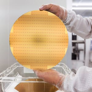
Nearly all microchips begin as slices of highly purified silicon.
 |Aug 7, 2023|
The terms “fab” and “foundry” are often used interchangeably, but that’s technically incorrect. Knowing the difference is important so you can better understand the semiconductor ecosystem.
 |Jun 7, 2023|
From the earliest chips to the latest technologies, silicon has long played a major role in semiconductor manufacturing as the substrates (wafers) on which devices are built.
 |May 10, 2023|
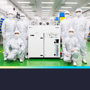
Lam Research has won a prestigious Edison Award for best new products in materials science. The bronze medal was awarded for our recently launched innovative suite of selective etch products...
 |Apr 5, 2023|
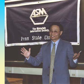
Hong Shih is one of 10 employees within the company who has been elevated to Lam Fellow He has more than 40 years of experience in sciences and engineering with over 30 years working in the...
 |Mar 7, 2023|
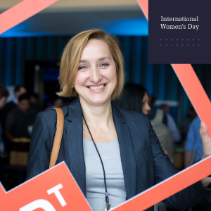
Gosia’s redirection in her studies resulted in a 20+ year long career in semiconductors A little bit of luck and a whole lot of talent got her to where she is today I sat down with Gosia...

 |Feb 16, 2023|
SEMICON Korea 2023 kicked off with a keynote speech, “Accelerating Innovation – From Lab to Fab,” delivered by Pat Lord, EVP of the Customer Support Business Group and Global Operations. Pat...