| Su | Mo | Tu | We | Th | Fr | Sa |
|---|---|---|---|---|---|---|
| Su | Mo | Tu | We | Th | Fr | Sa |
|---|---|---|---|---|---|---|


 |Mar 22, 2023|
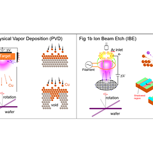
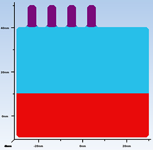
Introduction Cu’s resistivity depends on its crystal structure, void volume, grain boundaries and material interface mismatch, which becomes more significant at smaller scales. The formation of...
-
 |Mar 17, 2023|
System in Package (SiP) requirements push substrate designs to smaller features (similar to FO-PLP). Convergence in requirements allows shared R&D costs for panel level processing systems.


 |Mar 7, 2023|
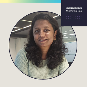
Women in Leadership at Lam has over 200 members Lam India has increased its diversity hiring percentages In recognition of International Women’s Day, Tina Correia, chief accounting officer, head...

 |Mar 7, 2023|
Gosia’s redirection in her studies resulted in a 20+ year long career in semiconductors A little bit of luck and a whole lot of talent got her to where she is today I sat down with Gosia...
 |Mar 3, 2023|
Soumya has automated Lam’s product software testing and processes for 19 years. The software she works on allows us to validate the behavior of our tool's software at any fab remotely. Soumya...

 |Feb 28, 2023|
With decreasing dynamic random-access memory (DRAM) cell sizes, DRAM process development has become increasingly difficult. Bit-line (BL) sensing margins and refresh times have become problematic...

 |Feb 16, 2023|
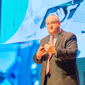
SEMICON Korea 2023 kicked off with a keynote speech, “Accelerating Innovation – From Lab to Fab,” delivered by Pat Lord, EVP of the Customer Support Business Group and Global Operations. Pat...

 |Feb 10, 2023|
Lam’s BEN ERG has grown by four times over a two-year period Our I&D actions and behaviors impact the communities where we live and work In recognition of Black History Month, Sherry Buie,...

 |Feb 2, 2023|
Metryx marked 200th tool shipment by donating science equipment to a local high school

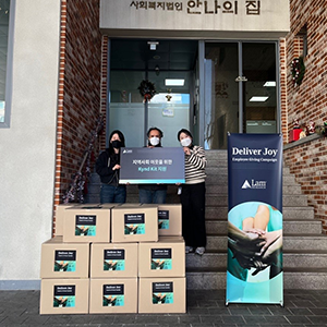 |Jan 20, 2023|
Nearly 2,000 employees participated in Deliver Joy programs, supporting 1,300 organizations More 10,640 volunteer hours were logged by our employees Deliver Joy in November and December is a...

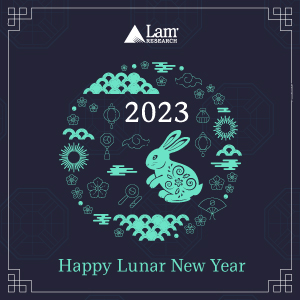 |Jan 18, 2023|
Sunday, January 22, marks the start of Lunar New Year. Across the world, including much of East Asia, nearly 1.5 billion people will ring in the Year of the Rabbit. According to the Chinese...

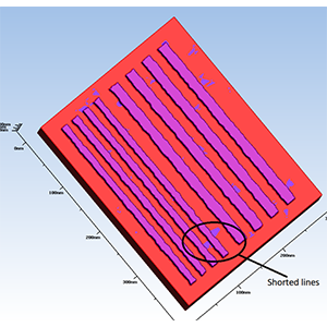 |Jan 13, 2023|
Line edge roughness (LER) can occur during the exposure step in lithography [1-2]. Similarly, etch and deposition process steps can leave a roughness on semiconductor surfaces. LER is a stochastic...

 |Dec 19, 2022|
At the beginning of my career in semiconductor equipment, the backside of the wafer was a source of anxiety. In one memorable instance in my early career, several wafers flew off a robot blade...

 |Dec 13, 2022|
Lam Japan has grown from nearly ten employees to over 500 in 30 years The company donated nearly $9,000 to local NGOs as part of the celebration Lam celebrated 30 years of operations in Japan on...
 |Dec 12, 2022|
Lam is once again named to the Dow Jones Sustainability Index for North America The company joins the UN Global Compact It’s been a year of progress as we march toward our goal to achieve net...
- |Nov 21, 2022|
“Engineering a Greener Fab” was the theme of the Lam Research Technical Symposium, Lam’s premiere forum for intellectual and scientific sharing.


 |Nov 11, 2022|
On November 11, we observe Veterans Day in the United States, an annual holiday recognizing those who have served in the armed forces and have made a significant commitment to their country. We...

 |Nov 9, 2022|
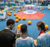
I was thrilled to attend the FIRST Global Challenge in Geneva in October, where Lam was a Gold Sponsor. The competition arena was full of high-school students, but I was the one who got an education.

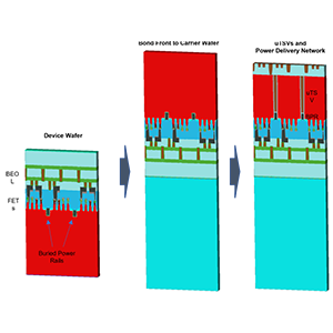
 |Nov 8, 2022|
Introduction The semiconductor industry has been focused on scaling and developing advanced technologies using advanced etch tools and techniques. With decreasing semiconductor device dimensions...
 |Nov 7, 2022|
12 suppliers were awarded 2022 Supplier Excellence awards Suppliers demonstrated success across three award categories: scaling, resiliency, and rapid prototype materials performance On Thursday,...

 Lam Research Drives Technology Advancements for Next-Generation Semiconductors (SEMICON Taiwan 2022)|Nov 2, 2022|
Lam Research was the platinum sponsor of the 27th gathering of SEMICON Taiwan, held September 14 to 16. More than 45,000 attendees examined 2,450 exhibition booths showing the latest industry...
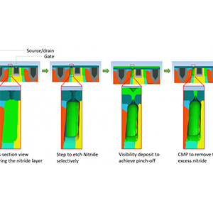 |Oct 27, 2022|
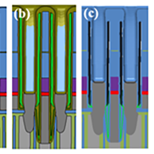
Reducing the parasitic capacitance between the gate metal and the source/drain contact of a transistor can decrease device switching delays. One way to reduce parasitic capacitance is to reduce...
 |Oct 17, 2022|
Lam launches 3-year partnership with FIRST Global to help inspire future innovators around the world Volunteers signed up to mentor robotics teams around the world for the FIRST Global Challenge...