| Su | Mo | Tu | We | Th | Fr | Sa |
|---|---|---|---|---|---|---|
| Su | Mo | Tu | We | Th | Fr | Sa |
|---|---|---|---|---|---|---|


 |Jun 16, 2022|
Chips are everywhere: from our mobile phones and automobiles to cloud servers for artificial intelligence, all of which seem to get faster, smarter, and better with each generation. Creating more...

 |Jun 1, 2022|
It takes a lot of different types of process tools to make chips, from deposition, to lithographic to etch and to cleaning tools among others. Large scale production requires chipmakers to use...

 |Mar 14, 2022|
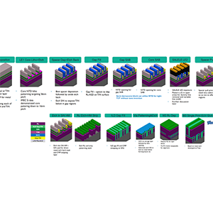
Introduction As we approach the 1.5nm node and beyond, new BEOL device integration challenges will be presented. These challenges include the need for smaller metal pitches, along with support for...

 |Feb 11, 2022|
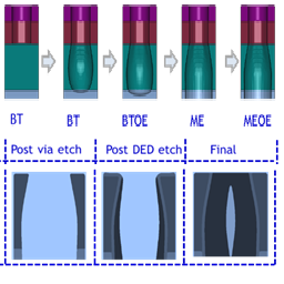
Design of Experiments (DOE) is a powerful concept in semiconductor engineering research and development. DOEs are sets of experiments used to explore the sensitivity of experimental variables and...

 |Feb 9, 2022|
Over the past decade, the need for increasingly smaller, denser, more powerful chips has been driving semiconductor manufacturers to move away from planar structures in favor of increasingly...

 |Feb 9, 2022|
Today, I am proud and excited to officially announce the availability of three new precision selective etch innovations from Lam Research: Argos®, Prevos™, and Selis®. Designed to complement...

 |Jan 4, 2022|
When I was a small child, I remember watching a 1966 American sci-fi adventure movie called “Fantastic Voyage” (the Korean title was “Micro Squad”) on an old black-and-white TV. The...

 |Dec 7, 2021|
The logic and memory chips that power our smart phones, laptops, gaming consoles and other favorite devices may be stealing all the headlines these days, but there are other types of...
-
|Dec 2, 2021|
For decades, the semiconductor industry has been defined by our ability to innovate. Each time we’ve been faced with seemingly insurmountable technological challenges, we have invented...

 |Oct 11, 2021|
The ability to process data is foundational to our smart, connected world. Microprocessors, in turn, rely on memory chips to store the data they need while working. One of the most popular types...

 |Sep 13, 2021|
Lam recently achieved an impressive product milestone with the shipment of our 10,000th single wafer clean chamber. This marks an incredible journey from the SP100 single chamber product first...

 |Aug 24, 2021|
We play a critical role in driving semiconductor breakthroughs for the next generation. Since 2015, Unlock Ideas has been an integral program to unleash the power of innovation by providing gifts...

 |Aug 16, 2021|
From August 23-27, our experts will join industry leaders at SEMICON Southeast Asia, to discuss semiconductor advancements in an era of 5G and next-generation technologies. Themed “Powering...

 |Aug 9, 2021|
As a materials engineer, I am very proud of the fact that key advances in human civilization have been driven by materials innovation. The stone age, bronze age and iron age were all essential...
 |Jul 26, 2021|
There’s a lot of talk about the Internet of Things (IoT) and its impact on our day-to-day lives. From home security systems to smart watches, IoT is upgrading the technologies we rely on every...

 |Jul 19, 2021|
Helium gas is increasingly in short supply. While consumers may be most familiar with it for use in filling balloons, it is used much more heavily in a variety of industrial processes –...

 |Jul 12, 2021|
Back in 1981, Lam pioneered single-wafer plasma etch tools with its first product, the Lam AutoEtch 480 plasma etcher. Introduced as “a streamlined plasma etching system designed specifically...
 |Jul 6, 2021|
The IEEE International Interconnect Technology Conference (IITC) will be held July 6-9, 2021, as a hybrid event – virtual and in-person (Kyoto Research Park, Kyoto, Japan), with on-demand...

 |Jun 21, 2021|
Preventative Maintenance “What is wet, but dry?” might sound like a riddle, and the answer for plasma process tools are “wet cleans,” an important type of preventative maintenance. The...
 |Jun 14, 2021|
Chip features continue to shrink to incredibly small dimensions and different device architectures are being devised to supply consumers with more powerful electronics. Atomic layer deposition...

 |Jun 7, 2021|
The pervasive use of technology has brought about a tremendous growth in data as well as an explosion in scaling and complexity of integrated circuits. That trend continues as the focus on...
 |Jun 1, 2021|
We take microprocessors for granted. Most people who aren’t deeply involved in technology may have no idea all of the places where a microprocessor shows up in their lives. It’s not just their...
 |May 24, 2021|
Engineers, scientists, and industry professionals will attend the 239th Electrochemistry Society (ECS) Meeting and the 18th International Meeting on Chemical Sensors (IMCS), held May 30 to June 3....

 |May 10, 2021|
Silicon chip manufacturing has always included etching as a critical processing step. But, increasingly, extremely high-aspect-ratio etching has been needed for 3D flash and DRAM chips, which have...

 |Mar 1, 2021|
As chipmakers move to advanced technology nodes, they are challenged to resolve ever finer features. One of the major roadblocks involves the material used to transfer chip design to the wafer;...
 |Feb 22, 2021|
Lam Research collaborates with universities and academic research consortia by supporting research, building relationships, and assisting graduate and undergraduate students with thesis awards,...
 |Feb 16, 2021|
The latest developments in patterning will be on stage at the upcoming SPIE Advanced Lithography, held as a digital forum February 22-26. Patterning – the set of steps that transfers chip...

 |Jan 27, 2021|
With more than a decade of industry leadership in high aspect ratio etching, Lam now introduces Vantex™, the latest in dielectric etch technology. Designed from the ground up specifically for...

 |Jan 19, 2021|
To kick-off the new year, SEMICON Korea is bringing together industry leaders throughout the semiconductor supply chain. Held February 3-12, participants can learn more about artificial...
 |Jan 4, 2021|
To kick-off the new year, we thought we’d share some of our favorite stories from 2020. While not exhaustive, this short list features articles that help put technology concepts into perspective...
 |Nov 30, 2020|
Filling complex, high aspect ratio structures is a challenge for 3D NAND, DRAM, and logic chipmakers. Lam’s Aaron Fellis, vice president and general manager of dielectric atomic layer deposition...
 |Oct 26, 2020|
When they were first commercialized at the 22 nm node, finFETs represented a revolutionary change to the way we build transistors, the tiny switches in the “brains” of a chip. As compared to...

 |Oct 19, 2020|
Semiconductor process development is no easy task, with each generation of devices more difficult and expensive to create. Traditional cycles of build-and-test development are becoming obsolete,...

 |Oct 12, 2020|
Lam’s newest product in its line of GAMMA® dry photoresist strip systems, brings the performance of the GAMMA® GxT® 300 mm to 200 mm wafer processing. The GAMMA GxT has been specifically...
 |Sep 21, 2020|
In today’s press release below, Lam announced the new Striker® FE platform featuring its patented ICEFill™ technology, which provides bottom-up filling in complex high aspect ratio (HAR)...

 |Sep 8, 2020|
Taiwan’s largest semiconductor convention is bringing together the industry’s brightest minds for a three-day exhibition. Held September 23-25 at the Taipei Nangang Exhibition Center, Hall 1...
 |Aug 10, 2020|
Diagnosis of any kind requires the synthesis of information. As humans we are much better at doing this when we have ways of visualizing information versus looking at numbers and statistics,...
 |Aug 3, 2020|
SEMICON Southeast Asia, the region’s premier electronics manufacturing supply chain exposition and conference, has gone virtual. Industry experts from around the world will share insights on...
 |Jul 27, 2020|
Lam CEO Tim Archer recently presented a compelling vision of the future at SEMICON West along with key industry leaders and influencers. Tim spoke of the pioneering work Lam Research has done over...
 |Jul 6, 2020|
The semiconductor industry’s flagship event, SEMICON West, is going virtual this year. Celebrating its 50th year, the show promises a full exhibition experience, featuring high level keynotes,...
 |Jun 30, 2020|
A key semiconductor trade show and forum, SEMICON China, was held June 27–29 at the Shanghai New International Expo Centre. Lam was pleased to be a sponsor of this event, which encompassed the...
-
|Jun 15, 2020|
The 20th International Conference on Atomic Layer Deposition (ALD 2020) featuring the 7th International Atomic Layer Etching Workshop (ALE 2020) will take place Monday, June 29–Wednesday, July...

 |May 28, 2020|
Lam Chief Technology Officer Rick Gottscho sat down with Semiconductor Engineering to share his insights on memory and equipment scaling, new market demands, and changes in manufacturing being...

 |May 11, 2020|
As integrated circuit designers bring more sophisticated chip functionality into smaller spaces, heterogeneous integration, including 3D stacking of devices, becomes an increasingly useful and...

 |Mar 16, 2020|
Lam Executive Vice President and Chief Technology Officer, Richard A. Gottscho, gave a keynote at the SEMI Industry Strategy Symposium (ISS), the annual executive conference for the semiconductor...

 |Mar 3, 2020|
Building on four decades of etch industry leadership, Lam today launched a new plasma etch technology and system solution. The new Sense.i™ platform features Lam’s Equipment Intelligence®...
 |Feb 26, 2020|
Addressing critical needs for next-generation device scaling, Lam today introduced a new dry photoresist technology that offers significant improvement in EUV lithography resolution, productivity...
-
|Feb 10, 2020|
The full spectrum of patterning topics will be discussed at the upcoming SPIE Advanced Lithography symposium. Held at the San Jose Convention Center on February 23-27, 2020, the event features...
 |Jan 13, 2020|
[Notice] SEMICON KOREA 2020 Is Canceled SEMICON Korea 2020, which was scheduled to be held from Feb 5 to Feb 7 by SEMI KOREA, will not take place as planned. You can find the details at the...
 |Jan 6, 2020|
2019 was quite a year for the Lam Blog. From sharing an inside peek at our favorite day of the year, Bring Our Children to Work Day, to showcasing our innovative technology and productivity...