| Su | Mo | Tu | We | Th | Fr | Sa |
|---|---|---|---|---|---|---|
| Su | Mo | Tu | We | Th | Fr | Sa |
|---|---|---|---|---|---|---|


 |Oct 19, 2023|
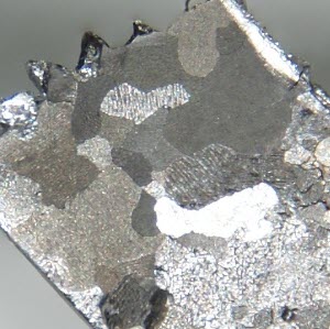
The semiconductor industry is searching for alternative metal line materials to replace copper due to the increasing barrier size and resistivity issues. Ruthenium (Ru) has shown promise as a potential replacement, outperforming copper and cobalt (Co) at smaller dimensions.

 |Sep 26, 2023|
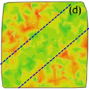
Virtual fabrication is a powerful tool to perform sensitivity analysis and provide guidance for inline process spec control
-
 |Sep 14, 2023|
Lam Research has supported the National GEM Consortium and GEM interns since 2019. Students who complete their fellowship have a chance to join Lam full-time.

 |Aug 31, 2023|
Video games and virtual and augmented reality are driving demand for haptics. Lam’s pulsed laser deposition capability can enable next-gen haptics technology.

 |Aug 23, 2023|
BEOL module processing faces challenges as chipmakers move to the 3 nm node and beyond. A semi-damascene integration scheme with airgap structures may help reduce RC delay time.

 |Aug 9, 2023|
Lam Research and the Centre for Nano Science and Engineering (CeNSE) at the Indian Institute of Science (IISc) partner to train up to 60,000 semiconductor engineers.

 |Jul 14, 2023|
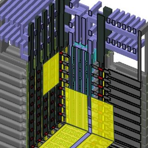
DRAM is following NAND in going 3D, but architecture needs are unique and challenging. 3D DRAM is needed to keep up with the demands of graphics cards, portable devices, and more. Here's an idea of how to architect it.

 |Jun 22, 2023|
Up to 60,000 engineers in India to be trained on Lam’s unique virtual fabrication platform
 |Jun 22, 2023|
New portfolio joins physical and virtual semiconductor worlds into a single ecosystem
-
 |Jun 20, 2023|
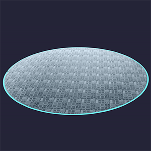
Addresses key manufacturing challenges and significantly improves wafer yield Builds on Lam's 15-year heritage of innovation in bevel solutions

 |Jun 14, 2023|
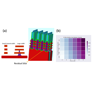
As transistor sizes shrink, short channel effects make it more difficult for transistor gates to turn a transistor ON and OFF [1]. One method to overcome this problem is to move away from planar...

 |May 30, 2023|
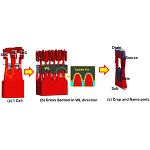
As DRAM technology nodes have scaled down, access transistor issues have been highlighted due to weak gate controllability. Saddle Fins with Buried Channel Array Transistors (BCAT) have...

 |May 25, 2023|
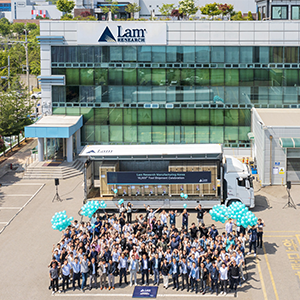
Achievement represents close collaboration with our customers and supply chain partners LMK joins Lam’s manufacturing operations in Livermore, Tualatin, and Taiwan in this milestone This week,...

 |May 2, 2023|
EVs can have almost twice as many microchips as combustion engine vehicles. Lam is a critical supplier for semiconductor manufacturers for EVs across all technologies.

 |Apr 13, 2023|
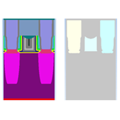
Introduction In logic devices such as FinFETs (field-effect transistors), metal gate parasitic capacitance can negatively impact electrical performance. One way to reduce this parasitic...
 |Apr 12, 2023|
The journal Nature publishes Lam’s groundbreaking study. Rick Gottscho and Keren Kanarik share what it means for Lam and the semiconductor industry.

 |Mar 22, 2023|
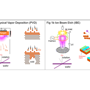
Introduction Cu’s resistivity depends on its crystal structure, void volume, grain boundaries and material interface mismatch, which becomes more significant at smaller scales. The formation of...
-
 |Mar 17, 2023|
System in Package (SiP) requirements push substrate designs to smaller features (similar to FO-PLP). Convergence in requirements allows shared R&D costs for panel level processing systems.

 |Mar 3, 2023|
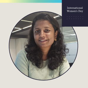
Soumya has automated Lam’s product software testing and processes for 19 years. The software she works on allows us to validate the behavior of our tool's software at any fab remotely. Soumya...

 |Feb 28, 2023|
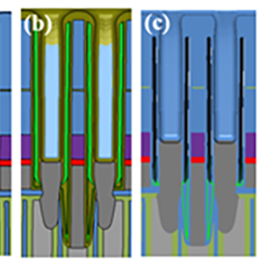
With decreasing dynamic random-access memory (DRAM) cell sizes, DRAM process development has become increasingly difficult. Bit-line (BL) sensing margins and refresh times have become problematic...

 |Feb 16, 2023|
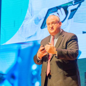
SEMICON Korea 2023 kicked off with a keynote speech, “Accelerating Innovation – From Lab to Fab,” delivered by Pat Lord, EVP of the Customer Support Business Group and Global Operations. Pat...
 |Feb 2, 2023|
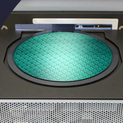
Metryx marked 200th tool shipment by donating science equipment to a local high school
 |Jan 13, 2023|
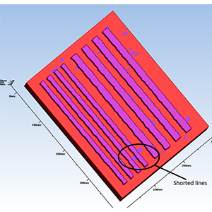
Line edge roughness (LER) can occur during the exposure step in lithography [1-2]. Similarly, etch and deposition process steps can leave a roughness on semiconductor surfaces. LER is a stochastic...

 |Dec 19, 2022|
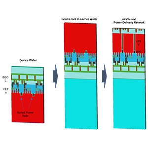
At the beginning of my career in semiconductor equipment, the backside of the wafer was a source of anxiety. In one memorable instance in my early career, several wafers flew off a robot blade...
- |Nov 21, 2022|
“Engineering a Greener Fab” was the theme of the Lam Research Technical Symposium, Lam’s premiere forum for intellectual and scientific sharing.