| Su | Mo | Tu | We | Th | Fr | Sa |
|---|---|---|---|---|---|---|
| Su | Mo | Tu | We | Th | Fr | Sa |
|---|---|---|---|---|---|---|


 |Dec 16, 2019|
The IoT and automotive markets use devices fabricated at a wide range of technology nodes. Taking advances made at 300 mm and applying them via upgrades to 200 mm equipment is a cost appropriate...

 |Dec 3, 2019|
Addressing the critical need for higher wafer edge yield, Lam has introduced new capabilities in its Corvus® etch and Coronus® plasma bevel clean systems. Chipmakers have long sought to overcome...

 |Nov 22, 2019|
It is an exciting time to be in the semiconductor industry and driving technology development which is fueling the intelligent, interconnected systems that will transform the way we work and live....

 |Nov 18, 2019|
Atomic layer etching and deposition processes offer atomic scale control through the use of self-limiting reactions. Yang Pan, corporate vice president of advanced technology development, shares...
 |Oct 30, 2019|
The SEMICON Europa tradeshow, the annual premier event for the global electronics industry in Europe, will take place November 12-15, 2019, at Messe München in Munich, Germany. The event connects...

 |Oct 28, 2019|
Moore’s Law has been the center of the semiconductor universe, dominated by a singular focus and a relentless drive to reduce transistor size and integrate more, smaller, faster transistors on...

 |Oct 24, 2019|
Technology experts and business leaders will be heading to the Advanced Semiconductor Technology Conference (ASTC) 2019, organized by SEMI Southeast Asia. Held November 7-8, 2019 at the Marina Bay...
 |Oct 7, 2019|
The science and technology of materials, interfaces, and processing will be in the spotlight at the AVS 66th International Symposium and Exhibition, being held October 20-25 in Columbus, Ohio....

 |Sep 30, 2019|
The 21st Semiconductor Exhibition (SEDEX) will be held this year at COEX in Seoul, Korea, October 8-11. The tradeshow will cover the full spectrum of the semiconductor industry supply chain; it...
 |Sep 30, 2019|
The fall meeting of the Electrochemical Society will be held October 13-17 in Atlanta, Georgia. A forum for the latest scientific and technical developments in both electrochemistry and solid...

 |Sep 9, 2019|
The largest microelectronics event in Taiwan is coming to TaiNEX this fall, welcoming more than 45,000 visitors from around the world. From September 18-20, leaders from the semiconductor industry...

 |Sep 3, 2019|
At an industry and investor event held during the August 2019 Flash Memory Summit, Lam management made the case for why semiconductor innovation needs to accelerate in the 5G era and how Lam is...
 |Aug 7, 2019|
With the introduction of two new products for 3D NAND manufacturing, Lam expands its stress management product portfolio. The VECTOR DT® PECVD and EOS® GS wet etch systems enable continued 3D...

 |Jul 15, 2019|
Food security is a growing concern. With the world’s population forecast to increase from 7.6 billion in 2017 to 9.8 billion by 2050, it’s estimated that an additional billion metric tons of...

 |Jul 12, 2019|
The rapid pace of semiconductor evolution places huge demands on the companies making the equipment used to build integrated circuits. With each new silicon node comes a host of new requirements,...
-
|Jul 8, 2019|
The AVS 19th International Conference on Atomic Layer Deposition (ALD 2019) featuring the 6th International Atomic Layer Etching Workshop (ALE 2019) will take place Sunday, July 21–Wednesday,...

 |Jun 24, 2019|
Gain insights, innovations, and intelligence in San Francisco this July 9-11 at the annual SEMICON West tradeshow. Industry leaders from around the world will gather for more than 80 hours of...
 |Jun 10, 2019|
Richard Gottscho, executive vice president and CTO of Lam Research, sat down with Semiconductor Engineering to talk about how to utilize more data from sensors in manufacturing equipment, the...
-
|May 13, 2019|
Electrochemistry and solid state science and technology will be featured at the 235th ECS Meeting, to be held May 26–30 in Dallas, Texas. Over the week, nearly two thousand talks will be given...

 |May 6, 2019|
Building semiconductors is an incredibly exacting process, with critical dimensions posing significant equipment challenges – and with the possibility that small process excursions can cause the...
 |Apr 29, 2019|
On May 7, 2019, semiconductor leaders and industry experts from around the world will convene at the Malaysia International Trade & Exhibition Centre (MITEC) in Kuala Lumpur, Malaysia to showcase...
 |Apr 24, 2019|
Addressing a need for self-maintaining semiconductor equipment, Lam has developed an etch productivity solution that extends the mean time between cleans (MTBC), a major limiter of etch system...

 |Mar 25, 2019|
More than most industries, ours is identified with a single element, silicon. Consider the self-adopted naming conventions of all the places that want to be recognized as members of the...
 |Mar 19, 2019|
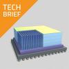
New sensing and actuating technologies for cars are introducing a new generation of 200 mm tools. Michelle Bourke, strategic marketing director in the customer support group, shares her thoughts...

 |Mar 4, 2019|
At this year’s SEMICON China, industry leaders from around the globe will come together for this fast-growing and dynamic microelectronics market to view products, technologies and brands that...
-
|Feb 11, 2019|
The SPIE Advanced Lithography symposium brings together leaders across the semiconductor industry to discuss the latest challenges in lithography and patterning. Held at the San Jose Convention...

 |Jan 22, 2019|
Our increasingly connected and ever “smarter” world generates increasing amounts of data, putting pressure on manufacturers who face new technical challenges in delivering the increasing...
 |Jan 10, 2019|
As one of the largest tradeshows and exhibitions in the region, SEMICON Korea brings together the best and the brightest of the semiconductor industry. Held from January 23 to January 25 at COEX,...
 |Jan 2, 2019|
Welcome back to the Lam Blog! To help start the new year, we want to share some of our favorite stories from 2018. Some of these articles highlight the driving forces in our industry, such as...
 |Dec 10, 2018|
Parents sharing stories about their childhoods and the miles of snow they had to walk through to get to school is not a new pastime. In fact, these anecdotes are often used to compare current...
 |Dec 3, 2018|
Robotics is the next technological revolution. Fiber optics, cables, and chips are shaping and directing our future. Here, we review some robotic milestones and take a peek into Lam’s commitment...
 |Nov 26, 2018|
The Electronics Packaging Technology Conference (EPTC 2018), an international event organized by the IEEE Reliability/CPMT/ED Singapore Chapter, will be held December 4–7 at the Resorts World...
 |Nov 12, 2018|
From November 13-16, the annual SEMICON Europa tradeshow will be at Messe München in Munich, Germany. Tens of thousands of highly influential industry attendees from around the world will convene...
 |Oct 29, 2018|
For hundreds of years, libraries have assembled and provided access to major written collections, serving as vital centers for those who thirst for knowledge. More recently, libraries have been...
-
|Oct 15, 2018|
The full semiconductor industry supply chain will be on display at the 20th Semiconductor Exhibition (SEDEX) at COEX in Seoul, Korea, October 24-26. The tradeshow will showcase memory, sensor,...
-
|Oct 8, 2018|
The AVS 65th International Symposium and Exhibition begins on October 21st in beautiful Long Beach, California. Scientists, engineers, and industry leaders from around the globe will gather to...
-
|Sep 24, 2018|
Starting on September 30, scientists, engineers, researchers, and industry professionals from around the globe will meet in Cancun, Mexico, at the Americas International Meeting on...
 |Sep 4, 2018|
Atomic layer etching (ALE) is one of the chipmaking processes that makes our data-driven world possible. After being confined to the laboratory for decades, ALE has awakened to become the most...
 |Aug 27, 2018|
This fall, SEMICON Taiwan, the largest microelectronics event in Taiwan, will welcome more than 40,000 visitors from around the globe. Taking place September 5-7 at the Taipei Nangang Exhibition...
 |Aug 13, 2018|
Electroplating is a common manufacturing process that applies a thin layer of one metal onto another. The U.S. penny, for example, has been made of zinc with a thin, electroplated coating of...
-
|Jul 23, 2018|
One of the most important conferences for the atomic layer processing community, the AVS 18th International Conference on Atomic Layer Deposition featuring the 5th International Atomic Layer...
 |Jul 2, 2018|
The big ideas shaping the world will be in the spotlight at SEMICON West, a premier microelectronics industry tradeshow. Held this year on July 11-13 in San Francisco, the show will feature...
 |Jun 21, 2018|
This month, copper interconnects turned 20. That’s probably something like 200 in “technology years” considering the pace of innovation today. Yet even after 20 years of advances in...
 |May 14, 2018|
Industry advancements and novel transformations in semiconductors will be addressed at SEMICON Southeast Asia 2018 from May 22-24 at the new Malaysia International Trade & Exhibition Centre...

 |Apr 16, 2018|
From PCRAM and MRAM to RRAM and more, there’s a whole new alphabet soup of memory technologies making their way to the fab. Fueling this development are technology advances in gaming and mobile...

 |Mar 5, 2018|
As one of the semiconductor industry’s largest annual tradeshow, SEMICON China is a great place to connect, collaborate, and innovate with the region’s growing chipmaking business. Attendees...
 |Feb 26, 2018|
Looking ahead into the new year in technology often proves quite interesting and educational. For 2018, one well-established market – automotive – is gaining the attention of many technology...
-
|Feb 20, 2018|
Continuing to make device components ever smaller and closely packed together is one of the challenges faced by the advanced patterning community every day. From February 25 to March 1, experts in...
 |Jan 22, 2018|
For more than thirty years, SEMICON Korea has been known as one of the largest semiconductor shows in the Korean semiconductor industry. This premier event for electronics manufacturing will...
 |Jan 16, 2018|
New semiconductor applications are ever changing and improving our lives, from new smartphones and wearables to healthcare, factory automation, and artificial intelligence. The humble memory chip...