| Su | Mo | Tu | We | Th | Fr | Sa |
|---|---|---|---|---|---|---|
| Su | Mo | Tu | We | Th | Fr | Sa |
|---|---|---|---|---|---|---|


 |Dec 4, 2017|
As a premier exposition for the electronics manufacturing supply chain, SEMICON Japan will brighten up Tokyo this December with the theme “dreams start here.” The SEMI tradeshows are each...

 |Oct 30, 2017|
For the first time, SEMICON Europa will be co-located with productronica – one of the world’s leading trade fairs for electronics development and production – at Messe München in Munich,...
 |Oct 23, 2017|
Some of the greatest minds in science and technology will be convening in Tampa for the 64th annual AVS International Symposium & Exhibition starting on October 29, 2017. Among the topics of...

 |Sep 25, 2017|
We often hear that advanced chips contain billions of transistors – an incredible, mind-blowing fact to be sure – but did you know that large-scale integrated chips (that are the size of a...
 |Sep 20, 2017|
Scientists, engineers, researchers, and industry professionals from around the globe will descend upon National Harbor, Maryland, this October to interact at the 232nd Electrochemical Society...

 |Sep 11, 2017|
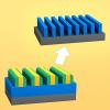
Multiple patterning continues to be an important technique for enabling pitch shrinking in advanced chip designs. However, as the number of steps grows, managing process variation is a key...
 |Sep 5, 2017|
The semiconductor manufacturing community is ready to connect at SEMICON Taiwan, the premier event for microelectronics manufacturing in Taiwan. This year, the event is expected to attract more...

 |Aug 28, 2017|
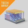
“Data is giving rise to a new economy” – The Economist (2017). This compelling reality makes the continued development of high-capacity data storage technologies like 3D NAND ever more...

 |Aug 7, 2017|
Chipmakers want every part of the wafer to produce, or yield, good die. Advances in process technologies over the years have just about made this a reality, even as feature dimensions continue to...
 |Jul 31, 2017|
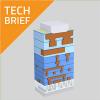
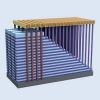
The industry’s transition to 3D NAND is being driven by several important advantages, including its ability to deliver higher capacity with a lower cost per bit. These vertical architectures...
-
|Jul 10, 2017|
The demands of our modern world for more connectivity, functionality, and capacity from our electronic devices – alongside the seemingly endless imagination for new applications – are pushing...
 |Jul 3, 2017|
If you’re part of the semiconductor industry, you know there are few better networking and technical sharing venues than the SEMICON tradeshows, and SEMICON West is no exception. Being held in...
 |Jun 12, 2017|
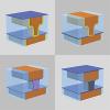
Used to extend the capabilities of conventional lithography, multiple patterning is a process of overlaying patterns of larger dimensions to achieve smaller and/or more tightly packed features. In...

 |May 15, 2017|
Imagine being able to deposit a film of material just a few atomic layers at a time. As impossible as that sounds, atomic layer deposition (ALD) is a reality. In fact, it’s being used in an...
 |Apr 10, 2017|
Southeast Asia is a major hub for the chip industry’s assembly, packaging, and test services – back-end manufacturing processes that are becoming an increasingly important topic of discussion....
 |Apr 7, 2017|
Panel-level fan-out chip manufacturing – using large square or rectangular substrates instead of wafers – is being developed as a means to lower the cost of back-end processes for some...
 |Mar 6, 2017|
In recent years, SEMICON China has become the semiconductor industry’s largest annual tradeshow, with much of its popularity likely due to the region’s growing chipmaking business. Attendees...

 |Feb 21, 2017|
It really is remarkable how our favorite tech products continue to become more compact and powerful, with today’s nanoscale chipmaking quite literally pushing the limits of what is possible. One...
 |Feb 6, 2017|
For its 30th anniversary, SEMICON Korea anticipates hosting its largest show ever, with an estimated 40,000 attendees converging at COEX in Seoul on February 8-10, 2017. Korea is the world’s...
 |Jan 17, 2017|
Ever open the body of your smartphone (perhaps unintentionally) and see small, black rectangles stuck on a circuit board? Those black rectangles are packaged chips. The external chip structure...
 |Dec 12, 2016|
This year marks the 40th anniversary for SEMICON Japan, one of the most extensive international exhibitions of semiconductor equipment and materials. Each SEMI tradeshow has its own unique...
 |Nov 28, 2016|
Did you know that different patterns require different types of multiple patterning? Today’s advanced chips are more complex than ever before, with transistors and other structures that are...

 |Nov 14, 2016|
Greek philosopher Democritus (460-370 BC) first proposed the existence of an ultimate particle, which he described as “atomos.” He probably never dreamed that one day there would be devices so...
-
|Nov 7, 2016|
State-of-the-art advances in plasma research and thin film science will be discussed at the AVS 63rd International Symposium and Exhibition, being held November 6-11 in Nashville, Tennessee. This...
-
|Sep 26, 2016|
Electrochemistry and solid-state science and technology will come together at the PRiME 2016 Meeting, held October 2-7 in Honolulu, Hawaii. One of the largest research conferences in the world,...

 |Sep 12, 2016|
Transistors are at the heart of our cherished electronics. Millions, or even billions, of these tiny switches go to work for us when we check our mobile phones, use our computers, start our...
 |Sep 6, 2016|
With the introduction of Lam’s latest Flex™ dielectric etch system, we have expanded our atomic layer etching (ALE) portfolio to include both conductor and dielectric etch. At the 10 nm...
 |Aug 29, 2016|
The semiconductor manufacturing community is gearing up for SEMICON Taiwan, the largest microelectronics event in Taiwan, which is expected to attract more than 40,000 visitors from around the...
 |Aug 9, 2016|
Addressing critical needs for next-generation 3D NAND and DRAM devices, Lam has developed the industry’s first all-atomic layer deposition (ALD) low-fluorine tungsten (LFW) fill process with its...
 |Aug 1, 2016|
Multiple patterning is an innovative approach to scaling semiconductors, but it also poses significant challenges controlling process variations. Lam’s Rick Gottscho, executive vice president of...
 |Jul 25, 2016|
Chip designs are changing. Features are shrinking to incredibly small dimensions and radically new device architectures are being devised to supply consumers with smaller, more powerful...
 |Jul 17, 2016|
The semiconductor industry has long relied on the development of innovative device architectures and technologies to continue device scaling. Making these a reality in production, however,...

 |Jul 11, 2016|
The semiconductor industry uses so many unique terms, it practically has its own language. To keep up on the latest developments, knowing that “language” can be really helpful. For instance,...
 |Jun 27, 2016|
What’s left after the relatively easy semiconductor manufacturing issues have been solved? The wicked hard problems – including things like scaling transistors down to 5 nm, reducing power...
 |Jun 19, 2016|
Industry experts came together recently to discuss some of the critical challenges facing interconnect scaling. As the number of transistors on advanced chips continues to increase, fabricating...
 |May 23, 2016|
Dave Hemker, CTO at Lam Research, sat down with Semiconductor Engineering to look at some of the key issues on the process and manufacturing side, and some of the key developments that will...
-
|May 16, 2016|
The continual scaling of device dimensions drives the need for ever smaller interconnects, the intricate wiring that links up to billions of individual components on a chip. As advanced devices...
 |Apr 25, 2016|
Building on its inaugural success last year, this year’s SEMICON Southeast Asia 2016 takes place April 26-28 at the SPICE Arena in Penang, Malaysia. Lam is pleased to be a premier sponsor of...

 |Apr 11, 2016|
Since its introduction in the 1980s, NAND flash memory has radically changed how we store our digital data. Remember ordering duplicate photos when getting camera film developed or burning your...
 |Mar 4, 2016|
The global semiconductor industry will be heading to the Shanghai New International Expo Centre for this year’s SEMICON China, which takes place March 15-17. Held in one of the largest and most...
 |Feb 29, 2016|
We often hear the word “inflection” used in the semiconductor industry, but what does it mean? In general, inflection refers to a point of change. In mathematics, for instance, an inflection...
-
|Feb 15, 2016|
Is Moore’s Law still on track? Can transistors, already more than a thousand times smaller than a grain of sand, continue to get even smaller? This is the challenge faced by the advanced...
 |Feb 1, 2016|
One of the most astounding aspects of semiconductor chips is their incredibly small scale. Practically measured in atoms, some feature dimensions are on the order of nanometers (nm) – that’s...
 |Jan 18, 2016|
With the new year underway, you may be wondering what lies ahead for the semiconductor world. Once again, Solid State Technology has checked in with industry leaders for their thoughts on the...
 |Jan 11, 2016|
From materials research to plasma fundamentals, Lam’s technologists are contributing to practical and theoretical developments in their fields. One way they help advance technology and expand...