| Su | Mo | Tu | We | Th | Fr | Sa |
|---|---|---|---|---|---|---|
| Su | Mo | Tu | We | Th | Fr | Sa |
|---|---|---|---|---|---|---|


 |Nov 16, 2023|
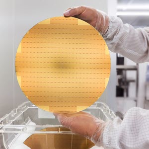
Nearly all microchips begin as slices of highly purified silicon.
 |Aug 7, 2023|
The terms “fab” and “foundry” are often used interchangeably, but that’s technically incorrect. Knowing the difference is important so you can better understand the semiconductor ecosystem.
 |May 10, 2023|
Lam Research has won a prestigious Edison Award for best new products in materials science. The bronze medal was awarded for our recently launched innovative suite of selective etch products...

 |Apr 5, 2023|
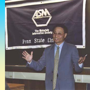
Hong Shih is one of 10 employees within the company who has been elevated to Lam Fellow He has more than 40 years of experience in sciences and engineering with over 30 years working in the...
 |Mar 7, 2023|
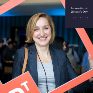
Gosia’s redirection in her studies resulted in a 20+ year long career in semiconductors A little bit of luck and a whole lot of talent got her to where she is today I sat down with Gosia...

 |Feb 16, 2023|
SEMICON Korea 2023 kicked off with a keynote speech, “Accelerating Innovation – From Lab to Fab,” delivered by Pat Lord, EVP of the Customer Support Business Group and Global Operations. Pat...

 Lam Research Drives Technology Advancements for Next-Generation Semiconductors (SEMICON Taiwan 2022)|Nov 2, 2022|
Lam Research was the platinum sponsor of the 27th gathering of SEMICON Taiwan, held September 14 to 16. More than 45,000 attendees examined 2,450 exhibition booths showing the latest industry...

 |Sep 8, 2022|
Calling all innovative entrepreneurs working on sustainability solutions The winner will be offered a $250,000 SAFE investment Theme is “Engineering a Greener Fab” Heatwaves such as the one...

 |Jul 21, 2022|
The electronics supply chain recently gathered together at SEMICON Southeast Asia, a premier event that promotes growth of the semiconductor and microelectronics ecosystem in the region. Held June...

 |Jul 12, 2022|
And yes, we’ve got a solution for that In the recent blog article Our wireless world – how Wi-Fi 6 will seamlessly integrate with 5G to keep us connected, David Haynes from our Customer...
 |Jul 7, 2022|
Lam Research will join fellow industry leaders from the extended electronics supply chain in a range of talks at the SEMICON West 2022 hybrid conference later this month. During the 52nd annual...

 |Jun 7, 2022|
Every few months, new and improved electronics are introduced. They’re typically smaller, smarter, faster, have more bandwidth, are more power-efficient, etc. – all thanks to a new generation...

 |Jun 1, 2022|
It takes a lot of different types of process tools to make chips, from deposition, to lithographic to etch and to cleaning tools among others. Large scale production requires chipmakers to use...
 |May 2, 2022|
David Haynes, vice president of Specialty Technologies for the Customer Support Business Group (CSBG) at Lam Research, discusses the introduction of Wi-Fi 6 and how, together with 5G, it will...
 |Nov 18, 2021|
Once considered to be science fiction and fodder for Hollywood films, artificial intelligence (AI) has become a near-ubiquitous technology in our communities, homes and workplaces that is helping...
 |Oct 11, 2021|
The ability to process data is foundational to our smart, connected world. Microprocessors, in turn, rely on memory chips to store the data they need while working. One of the most popular types...
 |Aug 9, 2021|
As a materials engineer, I am very proud of the fact that key advances in human civilization have been driven by materials innovation. The stone age, bronze age and iron age were all essential...
 |Jul 26, 2021|
There’s a lot of talk about the Internet of Things (IoT) and its impact on our day-to-day lives. From home security systems to smart watches, IoT is upgrading the technologies we rely on every...
 |Jun 1, 2021|
We take microprocessors for granted. Most people who aren’t deeply involved in technology may have no idea all of the places where a microprocessor shows up in their lives. It’s not just their...
 |Apr 26, 2021|
The excitement around the rollout of 5G technology could not be more palpable. We see this next-generation technology in news headlines and commercials, with promises to usher in the next wave of...
 |Jan 4, 2021|
To kick-off the new year, we thought we’d share some of our favorite stories from 2020. While not exhaustive, this short list features articles that help put technology concepts into perspective...

 |Nov 25, 2020|
The 22nd Electronics Packaging Technology Conference (EPTC) is going virtual this year. The flagship event of the IEEE Electronics Packaging Society (EPS) in Region 10 will highlight technical...
 |Nov 23, 2020|
The movement of money has undergone substantial changes over the years. With the advent of financial technology, or FinTech, the financial services industry has transformed. Enabled by today’s...
 |Oct 5, 2020|
Semiconductors can be considered as one of the most important inventions of all time. They are foundational to our ability to connect with each other; to collect, store and process information;...
 |Sep 28, 2020|
Cities around the globe are experiencing software updates – swapping out antiquated data collection techniques for new technological initiatives to promote efficiency, transparency, and...
 |Jul 29, 2020|
CMOS Image Sensor (CIS) technology has changed the way we interact with our devices and is expected to see significant growth in the market in the coming years. David Haynes, managing director of...
 |Jul 6, 2020|
The semiconductor industry’s flagship event, SEMICON West, is going virtual this year. Celebrating its 50th year, the show promises a full exhibition experience, featuring high level keynotes,...
 |Jun 22, 2020|
The medical space is constantly improving – experimenting and innovating to arrive at the most cutting-edge procedures. The past few decades have seen unprecedented advancements in medicine due...

 |May 28, 2020|
Lam Chief Technology Officer Rick Gottscho sat down with Semiconductor Engineering to share his insights on memory and equipment scaling, new market demands, and changes in manufacturing being...
 |May 4, 2020|
n 2019, 98.2 million viewers tuned in to watch the Superbowl, hailing the event as the “most viewed broadcast in America.” In recent years, a new player has emerged – eSports – bringing in...
 |Apr 27, 2020|
Have you ever seen a lightning bolt? What about the northern lights or a neon sign? These things are made of plasma, the fourth state of matter that makes up nearly 99.9% of the universe. In the...

 |Mar 23, 2020|
It’s pretty hard to talk about technology today without artificial intelligence, or AI, entering into the conversation. It seems to be everywhere… and growing. Businesses are using it to...

 |Mar 16, 2020|
Lam Executive Vice President and Chief Technology Officer, Richard A. Gottscho, gave a keynote at the SEMI Industry Strategy Symposium (ISS), the annual executive conference for the semiconductor...
 |Mar 2, 2020|
Augmented reality (AR) and virtual reality (VR) have unlocked incredible possibilities in education – bringing tomorrow’s technology into today’s learning. The influence of AR and VR...
 |Jan 6, 2020|
2019 was quite a year for the Lam Blog. From sharing an inside peek at our favorite day of the year, Bring Our Children to Work Day, to showcasing our innovative technology and productivity...
 |Dec 16, 2019|
The IoT and automotive markets use devices fabricated at a wide range of technology nodes. Taking advances made at 300 mm and applying them via upgrades to 200 mm equipment is a cost appropriate...

 |Dec 5, 2019|
For those of us in the semiconductor industry, the periodic table is more than just a poster on a science classroom wall: it’s a valuable resource that we use to create new logic and memory...
 |Nov 18, 2019|
Atomic layer etching and deposition processes offer atomic scale control through the use of self-limiting reactions. Yang Pan, corporate vice president of advanced technology development, shares...
 |Sep 16, 2019|
You don’t have to look very far in the semiconductor world before you see the word “scaling.” Perhaps you read an industry news article headline about transistor scaling – how those nearly...

 |Sep 3, 2019|
At an industry and investor event held during the August 2019 Flash Memory Summit, Lam management made the case for why semiconductor innovation needs to accelerate in the 5G era and how Lam is...
 |Jun 10, 2019|
Richard Gottscho, executive vice president and CTO of Lam Research, sat down with Semiconductor Engineering to talk about how to utilize more data from sensors in manufacturing equipment, the...
 |Jun 3, 2019|
Every industry has its unique lingo and the semiconductor industry is no different. Here, chips mean something a little different from our favorite snack and the word “fab” isn’t just used...

 |Mar 25, 2019|
More than most industries, ours is identified with a single element, silicon. Consider the self-adopted naming conventions of all the places that want to be recognized as members of the...

 |Mar 19, 2019|
New sensing and actuating technologies for cars are introducing a new generation of 200 mm tools. Michelle Bourke, strategic marketing director in the customer support group, shares her thoughts...
 |Feb 24, 2019|
Sensing technology, computing, and artificial intelligence (AI) are revolutionizing the skies. In recent years, the military has been applying drone technology to pave the way for the pilotless...
 |Jan 2, 2019|
Welcome back to the Lam Blog! To help start the new year, we want to share some of our favorite stories from 2018. Some of these articles highlight the driving forces in our industry, such as...
 |Sep 17, 2018|
This month, we celebrate the 60th anniversary of the integrated circuit (IC). On September 12, 1958, Jack Kilby produced a circuit containing both active and passive components fabricated from...

 |Aug 6, 2018|
Generations of humans have used varying methods to predict the weather. In the past, farmers thought rain was coming if their cows were lying down in the pasture. Today, things are a little more...
 |Jul 16, 2018|
Now that our time at SEMICON West 2018 is over, we’d like to reflect on some of the sound-bites overheard last week. As always, the three-day conference and expo gave us insights into today’s...
 |Jun 21, 2018|
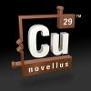
This month, copper interconnects turned 20. That’s probably something like 200 in “technology years” considering the pace of innovation today. Yet even after 20 years of advances in...