| Su | Mo | Tu | We | Th | Fr | Sa |
|---|---|---|---|---|---|---|
| Su | Mo | Tu | We | Th | Fr | Sa |
|---|---|---|---|---|---|---|


 |Sep 29, 2026|
Lam’s Semiverse Solutions team used digital twin modeling to explore a self-aligned CFET architecture that could help extend CMOS scaling beyond 10 Å.
-
 |Aug 25, 2026|
Lam Semiverse® Solutions engineers used SEMulator3D® stress modeling to show how channel thickness, fin width, and lateral etch can be optimized to reduce stress non-uniformity and improve gate-all-around nanosheet transistor performance.
-
 |Jul 30, 2026|
Learn how feedforward control helps semiconductor manufacturers reduce wafer scrap and improve yield. Semiverse Solutions simulation demonstrated a pass-rate increase from 60.82% to 96.77% through intelligent process correction.

 |Jun 29, 2026|
SEMulator3D virtual fabrication optimizes backside power networks by modeling nTSV-to-BPR connectivity.

 |Jun 16, 2026|
As AI accelerates demand for advanced chips, sustainability is becoming essential for long-term growth
-
 |Apr 27, 2026|
Pattern-dependent etch can lead to variations across the same chip. Dummy fill and SEMulator3D® help reduce shallow trench isolation and recess nonuniformity.
-
 |Mar 31, 2026|
In DRAM SAQP, small process variations can compound into pitch walk and, with LER, create line-bridge defects. Monte Carlo virtual fabrication reveals these interactions to tighten process windows and reduce wafer experimentation.

 |Mar 26, 2026|
Lam solutions for large 300-mm wafers aid in MEMS evolution. MEMS sensors are crucial in AI-powered devices and IoT. applications.

 |Feb 26, 2026|
SEMulator3D® Analytics is useful in calibrating FinFET device profiles, helping engineers achieve high precision in modeling fin etch depth and critical dimensions.
 |Nov 19, 2025|
Self-aligned backside contact (SABC) architectures in advanced GAA transistors expand the process window, reducing defects and improving chip yield.
 |Oct 31, 2025|
The article discusses the challenges and solutions for back-end-of-line (BEOL) patterning at the 3-nm semiconductor node, focusing on controlling critical process parameters to manage edge placement error (EPE) and critical dimension (CD) variability.

 |Oct 29, 2025|
Students at a growing number of U.S. schools learn the “why” of advanced 3D processes SEMulator3D® helps students with immersive training on leading edge technologies.
 |Oct 7, 2025|
Fabtex™ Yield Optimizer is a new Semiverse® Solutions product designed to improve yield and reduce process variability in high-volume semiconductor manufacturing.
-
 |Sep 30, 2025|
Virtual twins and process modeling speed up semiconductor development by simulating and optimizing designs before fabrication. This case study shows how to address etch uniformity issues from etch loading in slit patterns, enabling faster, more precise process optimization.
 |Sep 24, 2025|
Lam Research offers a range of advanced tools and technologies designed to support semiconductor manufacturing, focusing on precision, innovation, and improving chip production processes. These solutions include etch and deposition systems, process control tools, and software products aimed at next-generation device fabrication.

 |Aug 29, 2025|
Hybrid metallization using Mo is a promising alternative to conventional copper dual damascene.

 |Aug 5, 2025|
Lam Research is addressing critical challenges in the U.S. semiconductor industry by partnering with universities to enhance semiconductor engineering education through Semiverse® Solutions.
 |Jul 29, 2025|
Higher memory densities can be achieved with 3D NAND by increasing the number of metal and oxide layers. We looked at how to avoid tier bending and collapse that can accompany increasing layers using SEMulator3D.
 |Jul 2, 2025|
SEMulator3D® software is useful for semiconductor process modeling and virtual design Engineers can easily and vividly visualize complicated 3D structures with the tool Semiverse® Solutions,...
-
 |Jun 2, 2025|
Tiny changes in critical dimension, gate height, and similar features of advanced logic devices, such as FinFET SRAM, can affect yield. Through virtual experiments using the SEMulator3D® platform, the Semiverse Solutions team discusses how material stress and mechanical deformation resulting from these changes can be managed to enhance device performance.

 |Apr 30, 2025|
Ion Beam Etch (IBE) is a promising technology for extreme ultraviolet (EUV) lithography by significantly improving line edge roughness (LER) and line width roughness (LWR).

 |Feb 27, 2025|
DWMG structures can help improve DRAM by reducing energy waste. These structures fix a known flaw called “gate-induced drain leakage” (GIDL).
-
 |Jan 31, 2025|
To evaluate stress and mitigate its effects, predictive 3D process models can be used to predict the impact of mechanical stress on yield and performance.
 |Nov 20, 2024|
The latest advancements in semiconductor interconnect technologies, focusing on optimizing metal pitch structures for sub-2nm nodes.
-
 |Oct 24, 2024|
Intelligent machines enable faster design, production, maintenance, and process improvements. Numerous benefits can be gained from self-aware, self-maintained, and adaptive tools.
 |Sep 18, 2024|
By leveraging compact and neural network models, we predict capacitance performance with unprecedented accuracy.
 |Aug 27, 2024|
Digital twins help increase precision, affordability, sustainability, and speed-to-solution. Semiverse Solutions helps find the best process flow or recipe out of infinite combinations.

 |Jul 16, 2024|
On how to reduce transistor capacitance at the 5nm node using a source/drain contact recess.

 |Jun 20, 2024|
Abstract As conventional DRAM devices continue to shrink, increases in parasitic capacitance at smaller dimensions can negatively impact device performance.
-
 |May 14, 2024|
As semiconductor complexity increases with scaling, specialized expertise in areas like plasma physics and artificial intelligence (AI) becomes crucial. Lam faces challenges in workforce...
 |Apr 16, 2024|
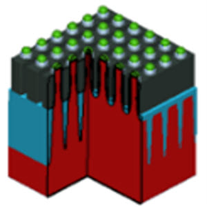
Abstract In this article, we demonstrate a pathfinding technique for a novel Vertical DRAM technology. First, we identify important process parameters (defined by current semiconductor production...

 |Apr 12, 2024|
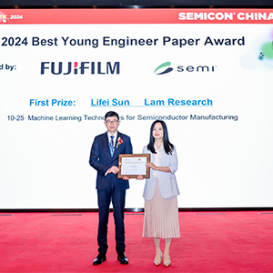
Li Fei Sun won for her paper on smart tools and ML solutions in semiconductor manufacturing In the past four years, Lam engineers have won the top award three times At Lam Research, we take pride...
-
 |Mar 21, 2024|
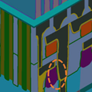
There are still many challenges to be overcome before CFET designs become mainstream, but this new 3D architecture represents a promising new direction for the future of computing.

 |Feb 22, 2024|
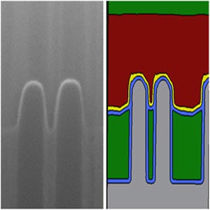
On the use and benefits of virtual fabrication in the development of DRAM saddle fin profiles
-
 |Jan 23, 2024|
We explore the causes and implications of asymmetric wafer defects in semiconductor manufacturing. We also consider the use of virtual process modeling to understand and mitigate these structural failures.
 |Dec 12, 2023|
The potential of Resistive Random Access Memory (ReRAM) as an alternative to SRAM for on-chip memory in advanced CPU applications.

 |Nov 20, 2023|
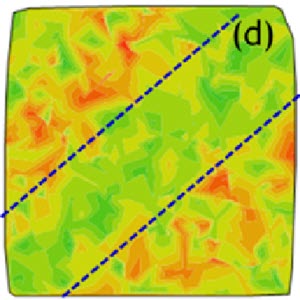
Virtual process development tools can accelerate the identification of process hotspots. These techniques lead to cost savings and improved yields in chip manufacturing.
 |Sep 26, 2023|
Virtual fabrication is a powerful tool to perform sensitivity analysis and provide guidance for inline process spec control
 |Aug 23, 2023|
BEOL module processing faces challenges as chipmakers move to the 3 nm node and beyond. A semi-damascene integration scheme with airgap structures may help reduce RC delay time.

 |Aug 9, 2023|
Lam Research and the Centre for Nano Science and Engineering (CeNSE) at the Indian Institute of Science (IISc) partner to train up to 60,000 semiconductor engineers.

 |Jul 14, 2023|
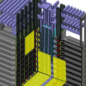
DRAM is following NAND in going 3D, but architecture needs are unique and challenging. 3D DRAM is needed to keep up with the demands of graphics cards, portable devices, and more. Here's an idea of how to architect it.
 |Jun 22, 2023|
Up to 60,000 engineers in India to be trained on Lam’s unique virtual fabrication platform
 |Jun 22, 2023|
New portfolio joins physical and virtual semiconductor worlds into a single ecosystem

 |Jun 14, 2023|
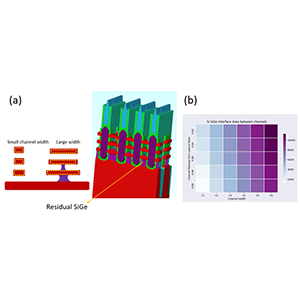
As transistor sizes shrink, short channel effects make it more difficult for transistor gates to turn a transistor ON and OFF [1]. One method to overcome this problem is to move away from planar...
 |May 30, 2023|
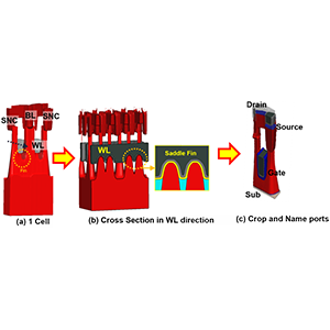
As DRAM technology nodes have scaled down, access transistor issues have been highlighted due to weak gate controllability. Saddle Fins with Buried Channel Array Transistors (BCAT) have...
 |Apr 13, 2023|
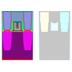
Introduction In logic devices such as FinFETs (field-effect transistors), metal gate parasitic capacitance can negatively impact electrical performance. One way to reduce this parasitic...
 |Mar 22, 2023|
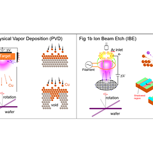
Introduction Cu’s resistivity depends on its crystal structure, void volume, grain boundaries and material interface mismatch, which becomes more significant at smaller scales. The formation of...
 |Feb 28, 2023|
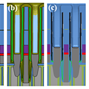
With decreasing dynamic random-access memory (DRAM) cell sizes, DRAM process development has become increasingly difficult. Bit-line (BL) sensing margins and refresh times have become problematic...

 |Feb 16, 2023|
SEMICON Korea 2023 kicked off with a keynote speech, “Accelerating Innovation – From Lab to Fab,” delivered by Pat Lord, EVP of the Customer Support Business Group and Global Operations. Pat...
 |Jan 13, 2023|
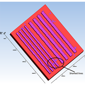
Line edge roughness (LER) can occur during the exposure step in lithography [1-2]. Similarly, etch and deposition process steps can leave a roughness on semiconductor surfaces. LER is a stochastic...